


Intel® PXA255 Processor Developer’s Manual 7-15
LCD Controller
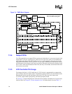
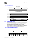
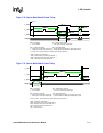
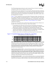
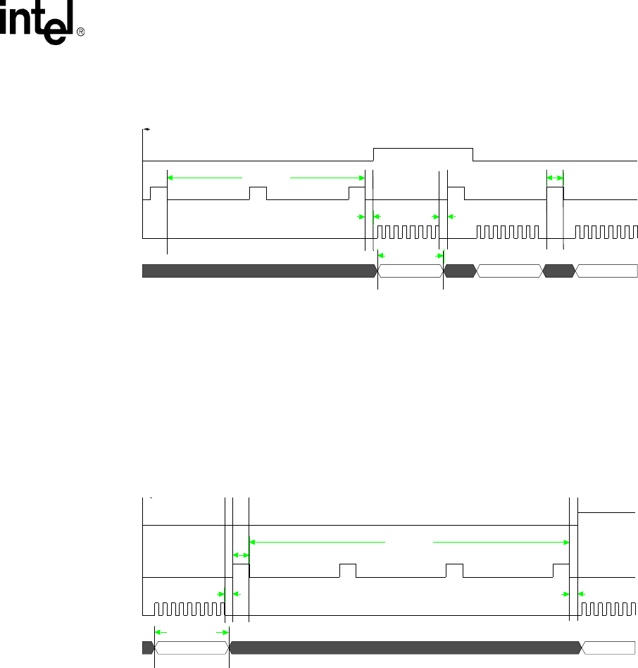
Figure 7-12. Passive Mode Start-of-Frame Timing
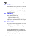
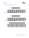
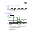
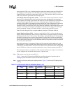
Figure 7-13. Passive Mode End-of-Frame Timing
Line 0 Data Line 1 Data Line 2 Data
PPL = 319
ELW = 0 ELW = 0 BLW = 0 BLW = 0
HSW = 1 HSW = 1 VSW = 1 VSW = 1
ENB - LCD Enable
0 - LCD is disabled
1 - LCD is enabled
VSP - Vertical Sync Polarity
0 - Frame clock is active high, inactive low
1 - Frame clock is active low, inactive high
HSP - Horizontal Sync Polarity
0 - Line clock is active high, inactive low
1 - Line clock is active low, inactive high
PCP - Pixel Clock Polarity
0 - Pixels sampled from data pins on rising edge of clock
1 - Pixels sampled from data pins on falling edge of clock
For PCP = 0 the L_PCLK waveform is inverted, but the timing is identical.
VSW = Vertical Sync Pulse Width - 1
HSW = Horizontal Sync (Line Clock) Pulse Width - 1
BLW = Beginning-of-Line Pixel Clock Wait Count - 1
ELW = End-of-Line Pixel Clock Wait Count - 1
L_FCLK
L_LCLK
L_PCLK
LDD[3:0]
ENB set to 1
PCP = 1
VSP = 0
HSP = 0
Line 239 Data Line 0 Data
PPL = 319
BLW = 0 BLW = 0 ELW = 0 ELW = 0
VSW = 2 VSW = 2
HSW = 1 HSW = 1
ENB - LCD Enable
0 - LCD is disabled
1 - LCD is enabled
VSP - Vertical Sync Polarity
0 - Frame clock is active high, inactive low
1 - Frame clock is active low, inactive high
HSP - Horizontal Sync Polarity
0 - Line clock is active high, inactive low
1 - Line clock is active low, inactive high
PCP - Pixel Clock Polarity
0 - Pixels sampled from data pins on rising edge of clock
1 - Pixels sampled from data pins on falling edge of clock
For PCP = 0 the L_PCLK waveform is inverted, but the timing is identical.
VSW = Vertical Sync Pulse Width - 1
HSW = Horizontal Sync (Line Clock) Pulse Width - 1
BLW = Beginning-of-Line Pixel Clock Wait Count - 1
ELW = End-of-Line Pixel Clock Wait Count - 1
PPL = Pixels Per Line - 1
L_FCLK
L_LCLK
L_PCLK
LDD[3:0]
ENB
set
to
1
PCP = 1
VSP = 0
HSP = 0
LPP = Lines Per Panel - 1
LPP = 239