


Intel® PXA255 Processor Developer’s Manual 6-21
Memory Controller
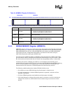
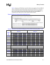
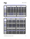
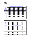
2x13x8x32 24 23 22 21 20 19 18 17 16 15 14 13 12 11 10 24 23 ‘0’ 98765432
2x13x8x16 23 22 21 20 19 18 17 16 15 14 13 12 11 10 9 23 22 ‘0’ 87654321
2x13x9x32 25 24 23 22 21 20 19 18 17 16 15 14 13 12 11 25 24 ‘0’ 10 98765432
2x13x9x16 24 23 22 21 20 19 18 17 16 15 14 13 12 11 10 24 23 ‘0’ 987654321
2x13x10x32 NOT VALID (too big) NOT VALID (too big)
2x13x10x16 25 24 23 22 21 20 19 18 17 16 15 14 13 12 11 25 24 ‘0’ 10 987654321
2x13x11x32 NOT VALID (too big) NOT VALID (too big)
2x13x11x16 NOT VALID (too big) NOT VALID (too big)
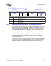
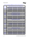
Table 6-8. External to Internal Address Mapping for SA-1111 Addressing (Sheet 1 of 3)
# Bits
Bank x
Row x
Col x
Data
External Address pins at SDRAM RAS Time
MA<24:10>
External Address pins at SDRAM CAS Time
MA<24:10>
24 23 22 21 20 19 18 17 16 15 14 13 12 11 10 24 23 22 21 20 19 18 17 16 15 14 13 12 11 10
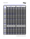
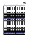
1x11x8x32 21 20 19 18 17 16 15 14 13 12 11 10 21 ‘0’ 9 8 7 6 5 4 3 2
1x11x8x16 NOT VALID (illegal addressing combination) NOT VALID (illegal addressing combination)
1x11x9x32 21 20 19 18 17 16 15 14 13 12 11 10 21 ‘0’ 22 9 8 7 6 5 4 3 2
1x11x9x16 21 20 19 18 17 16 15 14 13 12 11 10 21 ‘0’ 9 8 7 6 5 4 3 2 1
1x11x10x32 21 20 19 18 17 16 15 14 13 12 11 10 21 ‘0’ 23 22 9 8 7 6 5 4 3 2
1x11x10x16 21 20 19 18 17 16 15 14 13 12 11 10 21 ‘0’ 22 9 8 7 6 5 4 3 2 1
1x11x11x32 NOT VALID (illegal addressing combination) NOT VALID (illegal addressing combination)
1x11x11x16 NOT VALID (illegal addressing combination) NOT VALID (illegal addressing combination)
1x12x8x32 22 21 20 19 18 17 16 15 14 13 12 11 10 21 ‘0’ 9 8 7 6 5 4 3 2
1x12x8x16 NOT VALID (illegal addressing combination) NOT VALID (illegal addressing combination)
1x12x9x32 22 21 20 19 18 17 16 15 14 13 12 11 10 21 ‘0’ 23 9 8 7 6 5 4 3 2
1x12x9x16 22 21 20 19 18 17 16 15 14 13 12 11 10 21 ‘0’ 9 8 7 6 5 4 3 2 1
1x12x10x32 22 21 20 19 18 17 16 15 14 13 12 11 10 21 ‘0’ 24 23 9 8 7 6 5 4 3 2
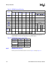
Table 6-7. External to Internal Address Mapping for Normal Bank Addressing (Sheet 3 of 3)
# Bits
Bank x
Row x
Col x
Data
External Address pins at SDRAM RAS Time
MA<24:10>
External Address pins at SDRAM CAS Time
MA<24:10>
24 23 22 21 20 19 18 17 16 15 14 13 12 11 10 24 23 22 21 20 19 18 17 16 15 14 13 12 11 10