Intel® PXA255 Processor Developer’s Manual 6-17
Memory Controller
6.5.4 Fixed-Delay or Return-Clock Data Latching
The Return-clock data latching works in all situations. Fixed-delay latching is not guaranteed to
work in all situations and must not be used. Fixed-delay latching does not work all the time because
the delays through the output pads can vary widely over a range of conditions. Because this delay
can be greater than a clock cycle, it is impossible to determine the clock to latch the data from the
SDRAM. Program the MDCNFG:DLATCHx and SXCNDF:SXLATCHx fields to a 1 to enable
latching using the return clock SDCLK.
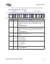
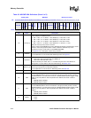
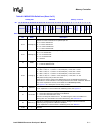
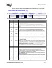
13 K0RUN
Synchronous Static Memory Clock Run Pin 0 (SDCLK<0>) Control/Status
0 – SDCLK0 is disabled
1 – SDCLK0 is enabled
Set on exit from hardware and sleep reset if the BOOT_SEL signals are configured for a
synchronous memory type.
K0RUN can be cleared by the program, but this capability must be used with caution
because the resulting state prohibits automatic transitions for any commands.
12 E0PIN
Synchronous Static Memory Clock Enable Pin 0 (SDCKE<0>) Level Control/Status
0 – SDCKE0 is disabled
1 – SDCKE0 is enabled
This bit is set on exit from hardware and sleep reset if the BOOT_SEL signals are
configured for a synchronous memory type.
E0PIN can be cleared by the program to cause a power-down command (if K0RUN=1).
Use with caution because the resulting state prohibits automatic transitions for Mode
Register Set command and read commands. E0PIN can be set by the program to cause a
power-down-exit command (if K0RUN=1).
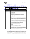
11:0 DRI
SDRAM refresh interval, all partitions.
The number of memory clock cycles divided by 32 between auto refresh (CBR) cycles. One
row is refreshed in each SDRAM bank during each CBR refresh cycle. This interval is
applicable to all SDRAM in the four partitions. To calculate the refresh interval from this
programmed number, 31 is added to this number after it is multiplied by 32.
The value that must be loaded into this register is calculated as follows:
DRI = (Number of memclk cycles-31) / 32 =
(Refresh time / rows) x Memory clock frequency / 32.
Must be programmed to be shared by both partition pairs. The smallest number must be
programmed.
Must be less than the tRAS (max) for the SDRAM being accessed.
When cleared to 0, no refreshes are sent to the SDRAMs.
If all four SDRAM partitions are disabled, the refresh counter is disabled and refreshes are
only performed when a single transaction to a disabled SDRAM partition is requested.
If the clock frequency is changed, this register must be rewritten, even if the value has not
changed. This results in a refresh and the refresh counter is reset to the refresh interval.
The minimum value that the MDREFR[DRI] bit can be set to is 0x13.
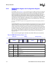
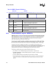
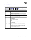
Table 6-5. MDREFR Bit Definitions (Sheet 3 of 3)
0x4800_0004 MDREFR Memory Controller
Bit
31 30 29 28 27 26 25 24 23 22 21 20 19 18 17 16 15 14 13 12 11 10 9 8 7 6 5 4 3 2 1 0
reserved
K2FREE
K1FREE
K0FREE
SLFRSH
reserved
APD
K2DB2
K2RUN
K1DB2
K1RUN
E1PIN
K0DB2
K0RUN
E0PIN
DRI
Reset
0 0 0 0 0 0 1 1 1 1 0 0 1 0 1 0 0 1 * * 1 1 1 1 1 1 1 1 1 1 1 1
Bits Name Description


