


Intel® PXA255 Processor Developer’s Manual 6-57
Memory Controller
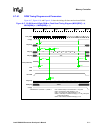
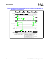
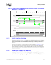
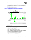
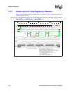
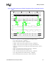
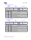
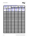
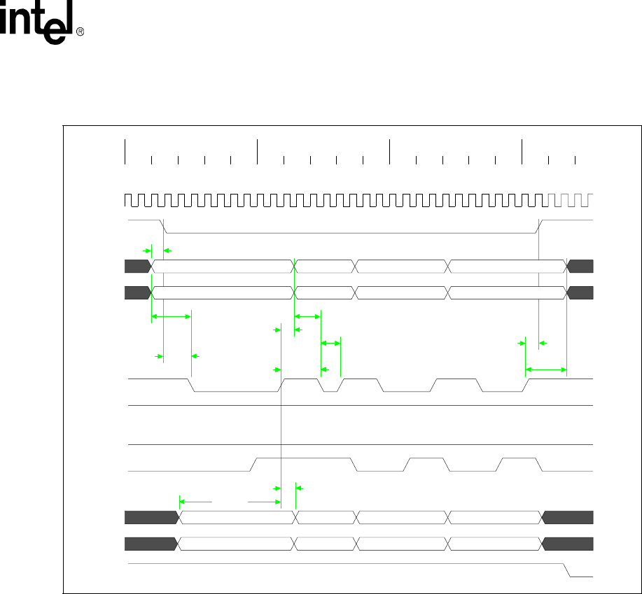
In Figure 6-21 and Figure 6-22, some of the parameters are defined as follows:
• tAS = Address setup to nCS = 1 MEMCLK
• tCES = nCS setup to nOE or nPWE = 2 MEMCLKs
• tASRW0 = Address setup to nOE or nPWE low (asserted) = 3 MEMCLKs
• tASRWn = Address setup to nOE or nPWE low (asserted) = RDN MEMCLKs
• tDSWH,min = Minimum write data, DQM setup to nPWE high (deasserted) = (RDF+2)
MEMCLKs
• tDHW = Data, DQM hold after nPWE high (deasserted) = 1 MEMCLK
• tDHR = Data hold required after nOE deasserted = 0 ns
• tCEH = nCS held asserted after nOE or nPWE deasserted = 1 MEMCLK
• tAH = Address hold after nOE or nPWE deasserted = 1 MEMCLK
• nOE or nPWE high time between burst beats = (RDN+2) MEMCLKs
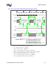
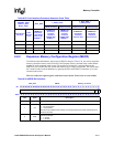
Figure 6-22. 32-Bit Variable Latency I/O Write Timing (Burst-of-Four, Variable Wait Cycles Per
Beat)
0 1 2 3
byte addr byte addr byte addr byte addr
D0 D1 D2 D3
mask0 mask1 mask2 mask3
tDH
tDSWH
tCEH
RRR*2+1
RDF+1+Waits
RDN+2
tASWN
RDF+1+Waits
RDN+
tAH
tASRW0
tCES
tAS
MEMCLK
nCS[0]
MA[25:2]
MA[1:0]
nPWE
nOE
RDnWR
RDY
MD[31:0]
DQM[3:0]
nCS[1]