


4-12 Intel® PXA255 Processor Developer’s Manual
System Integration Unit
4.1.3.4 GPIO Rising Edge Detect Enable Registers (GRER0, GRER1, GRER2)
and Falling Edge Detect Enable Registers (GFER0, GFER1, GFER2)
Each GPIO can also be programmed to detect a rising-edge, falling-edge, or either transition on a
pin. When an edge is detected that matches the type of edge programmed for the pin, a status bit is
set. The interrupt controller can be programmed so that an interrupt is signalled to the core when
any of these status bits are set. Additionally, the interrupt controller can be programmed so that a
subset of the status bits causes the processor to wake from Sleep mode when they are set. Refer to
Section 3.4.9, “Sleep Mode” on page 3-15 and Section 3.5.6, “Power Manager GPIO Edge Detect
Status Register (PEDR)” on page 3-28 for more information on which status bits can cause a wake
up from Sleep mode.
Use the GRER and the GFER to select the type of transition on a GPIO pin that causes a bit within
the GPIO Edge Detect Enable Status register (GEDR) to be set. For a given GPIO pin, its
corresponding GRER bit is set causing a GEDR status bit to be set when the pin transitions from
logic level zero to logic level one. Likewise, the GFER is used to set the corresponding GEDR
status bit when a transition from logic level one to logic level zero occurs. When the corresponding
bits are set in both registers, either a falling- or a rising-edge transition causes the corresponding
GEDR status bit to be set.
Note: The minimum pulse width duration to guarantee edge detection is 1µS.
Table 4-15 through Table 4-17 show the bitmaps of the GRER0, GRER1, and GRER2. Table 4-18
through Table 4-20 show the bitmaps of the GFER, GFER1, and GFER2.
Note: For reserved bits in GRER2 and GFER2, writes must be zeros and reads must be ignored.
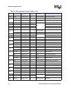
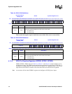
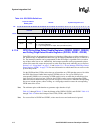
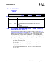
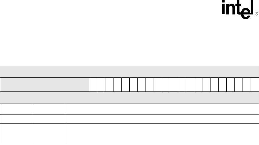
Table 4-14. GPCR2 Bit Definitions
Physical Address
0x40E0_002C
GPCR2 System Integration Unit
Bit
31 30 29 28 27 26 25 24 23 22 21 20 19 18 17 16 15 14 13 12 11 10 9 8 7 6 5 4 3 2 1 0
reserved
PC84
PC83
PC82
PC81
PC80
PC79
PC78
PC77
PC76
PC75
PC74
PC73
PC72
PC71
PC70
PC69
PC68
PC67
PC66
PC65
PC64
Reset 0 0 0 0 0 0 0 0 0 0 0 0 0 0 0 0 0 0 0 0 0 0 0 0 0 0 0 0 0 0 0 0
Bits Name Description
<31:21> — reserved
<20:0> PC[x]
GPIO Pin ‘x’ Output Pin Clear (where x= 64 through 84).
0 – Pin level unaffected.
1 – If pin configured as an output, clear pin level low (zero).