16-18 Intel® PXA255 Processor Developer’s Manual
Network SSP Serial Port
16.5 Register Descriptions
Each SSP consists of seven registers: three control, one data, one status, one time-out, and one test.
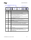
• The SSP control registers (SSCR0, SSCR1) configure the baud rate, data length, frame format,
data-transfer mechanism, and port enabling. They also permit setting the FIFO trigger
threshold that triggers an interrupt.
• Access all registers using aligned words.
Note: Write the SSP registers after a reset but before the SSP is enabled.
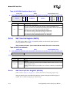
• The SSP Time-Out (SSTO) register programs the time-out value used to signal a specified
period of receive FIFO inactivity.
• While in PSP mode, the SSP Programmable Serial Protocol (SSPSP) register programs the
parameters used in defining the data transfer.
• The data register is mapped as one 32-bit location, which physically points to either of two 32-
bit registers: one register is for writes of data transfers to the transmit FIFO and the other
register is for reads that take data from the receive FIFO. A write cycle or burst write puts
successive words into the SSP write register and then into the transmit FIFO. A read cycle or
burst read takes data from the SSP read register and the receive FIFO reloads it with available
data bits it has stored.
Do not increment the address using read and write DMA bursts.
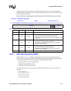
• Besides showing the state of the FIFO buffers, the status register shows whether the
programmable trigger threshold has been passed and whether a transmit or receive FIFO
service request is active. The status register also shows how full the FIFO is. Flag bits indicate
when the SSP is actively transmitting data, when the transmit FIFO is not full, and when the
receive FIFO is not empty. The SSSR[ROR] bit signals an overrun of the receive FIFO In this
case newly received data is discarded.
When programming registers, reserved bits must be written as zeroes and read as undefined.
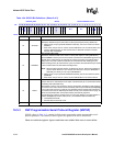
16.5.1 SSP Control Register 0 (SSCR0)
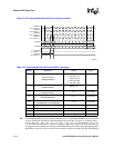
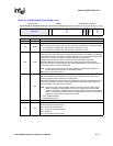
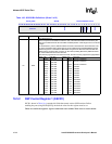
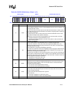
SSCR0, shown in Table 16-3, contains bit fields that control various functions within the SSP.
Before enabling the SSP (via SSE) the desired values for this register must be set.
These are read/write registers. Ignore reads from reserved bits. Write zeros to reserved bits.


