


Intel® PXA255 Processor Developer’s Manual 2-9
System Architecture
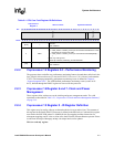
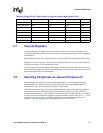
Table 2-6 describes the PXA255 processor pins.
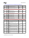
IA Analog Input
OA Analog output
IAOA Analog bidirectional
SUP Supply pin (either VCC or VSS)
Table 2-5. Processor Pin Types
Type Function
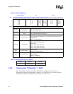
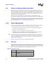
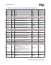
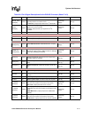
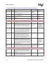
Table 2-6. Pin & Signal Descriptions for the PXA255 Processor (Sheet 1 of 9)
Pin Name Type Signal Descriptions Reset State Sleep State
Memory Controller Pins
MA[25:0] OCZ
Memory address bus. (output) Signals the address
requested for memory accesses.
Driven Low Driven Low
MD[15:0] ICOCZ
Memory data bus. (input/output) Lower 16 bits of the
data bus.
Hi-Z Driven Low
MD[31:16] ICOCZ
Memory data bus. (input/output) Used for 32-bit
memories.
Hi-Z Driven Low
nOE OCZ
Memory output enable. (output) Connect to the output
enables of memory devices to control data bus drivers.
Driven High Note [4]
nWE OCZ
Memory write enable. (output) Connect to the write
enables of memory devices.
Driven High Note [4]
nSDCS[3:0] OCZ
SDRAM CS for banks 3 through 0. (output) Connect to
the chip select (CS) pins for SDRAM. For the PXA255
processor nSDCS0 can be Hi-Z, nSDCS1-3 cannot.
Driven High Note [5]
DQM[3:0] OCZ
SDRAM DQM for data bytes 3 through 0. (output)
Connect to the data output mask enables (DQM) for
SDRAM.
Driven Low Driven Low
nSDRAS OCZ
SDRAM RAS. (output) Connect to the row address
strobe (RAS) pins for all banks of SDRAM.
Driven High Driven High
nSDCAS OCZ
SDRAM CAS. (output) Connect to the column address
strobe (CAS) pins for all banks of SDRAM.
Driven High Driven High
SDCKE[0] OC
Synchronous Static Memory clock enable. (output)
Connect to the CKE pins of SMROM. The memory
controller provides control register bits for deassertion.
Driven Low Driven Low
SDCKE[1] OC
SDRAM and/or Synchronous Static Memory clock
enable. (output) Connect to the clock enable pins of
SDRAM. It is deasserted during sleep. SDCKE[1] is
always deasserted upon reset. The memory controller
provides control register bits for deassertion.
Driven Low Driven Low
SDCLK[0] OC
Synchronous Static Memory clock. (output) Connect to
the clock (CLK) pins of SMROM. It is driven by either the
internal memory controller clock, or the internal memory
controller clock divided by 2. At reset, all clock pins are
free running at the divide by 2 clock speed and may be
turned off via free running control register bits in the
memory controller. The memory controller also provides
control register bits for clock division and deassertion of
each SDCLK pin. SDCLK[0] control register assertion bit
defaults to on if the boot-time static memory bank 0 is
configured for SMROM.