6-44 Intel® PXA255 Processor Developer’s Manual
Memory Controller
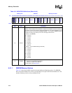
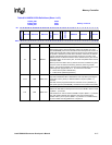
The RT fields in the MSCx registers specify the type of memory:
• Non-burst ROM or Flash
• SRAM
• Variable Latency I/O
• Burst-of-four ROM or Flash
• Burst-of-eight ROM or Flash
The RBW fields specify the bus width for the memory space selected by nCS[5:0]. For a 16-bit bus
width transactions occur on MD[15:0]. The BOOT_SEL pins and/or SXCNFG register must be
used to configure nCS[3:0] for SMROM or some other type of Synchronous Static Memory.
6.7.2 Static Memory SA-1111 Compatibility Configuration
Register (SA1111CR)
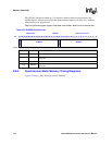
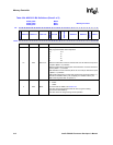
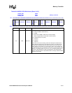
The SA1111CR register was added to the PXA255 processor to facilitate interfaces that behave
differently based upon the size of the transfer requested, such as a PCI bridge. Normally, when an 8
or 16 bit read is requested, the PXA255 processor asserts all DQM signals and sets the lowest
address pins (MA[1:0] for 32 bit external bus and MA[0] for 16 bit external bus) to zero and
discards the unwanted portion of data. When the SA-1111 compatibility bit is set for a static
memory partition, then two things will happen.
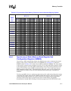
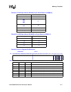
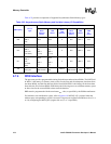
• First, on reads for asynchronous memory, the lower address bits will correctly reflect the
starting byte address. This is MA[0] for 16-bit external memory and MA[1:0] for 32-bit
external memory. This is based on the byte enables that may be associated with the read
request from the internal bus. See
Table 6-21, “32-Bit Byte Address Bits MA[1:0] for Reads
Based on DQM[3:0]” and Table 6-22, “16-Bit Byte Address Bit MA[0] for Reads Based on
DQM[1:0]” for specifics on the external address for this mode.
• Second, on reads, the DQM pins will correctly reflect the byte enables received for the reads.
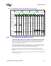
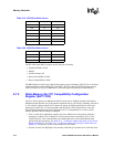
Table 6-19. 32-Bit Bus Write Access
Data Size MA[1:0] DQM[3:0]
8-bit 00 1110
8-bit 01 1101
8-bit 10 1011
8-bit 11 0111
16-bit 00 1100
16-bit 10 0011
32-bit 00 0000
Table 6-20. 16-Bit Bus Write Access
Data Size MA[0] DQM[1:0]
8-bits 0 10
8-bits 1 01
16-bits 0 00


