


6-60 Intel® PXA255 Processor Developer’s Manual
Memory Controller
6.8 16-Bit PC Card/Compact Flash Interface
The following sections provide information on the card interface based on the PC Card Standard -
Volume 2 - Electrical Specification, Release 2.1, and CF+ and CompactFlash Specification
Revision 1.4. Only 8- and 16-bit data transfers are supported.
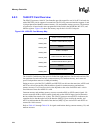
6.8.1 Expansion Memory Timing Configuration Register
MCMEM0, MCMEM1, MCATT0, MCATT1, MCIO0, and MCIO1 are read/write registers that
contain control bits for configuring the timing of the 16-bit PC Card/Compact Flash interface.
The programming of each of the four fields in each of the six registers lets software to individually
select the duration of accesses to I/O, common memory, and attribute space for each of two 16-bit
PC Card/Compact Flash card slots.
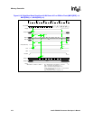
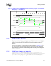
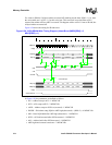
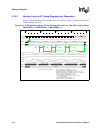
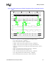
Refer to Table 6-26 through Table 6-28 for bitmaps of the MCMEMx registers. Also refer to
Table 6-29. Refer to Figure 6-29 and Figure 6-30 for a 16-bit PC Card/Compact Flash timing
diagram.
These are read/write registers. Ignore reads from reserved bits. Write zeros to reserved bits.
These are read/write registers. Ignore reads from reserved bits. Write zeros to reserved bits.
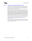
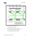
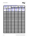
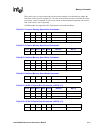
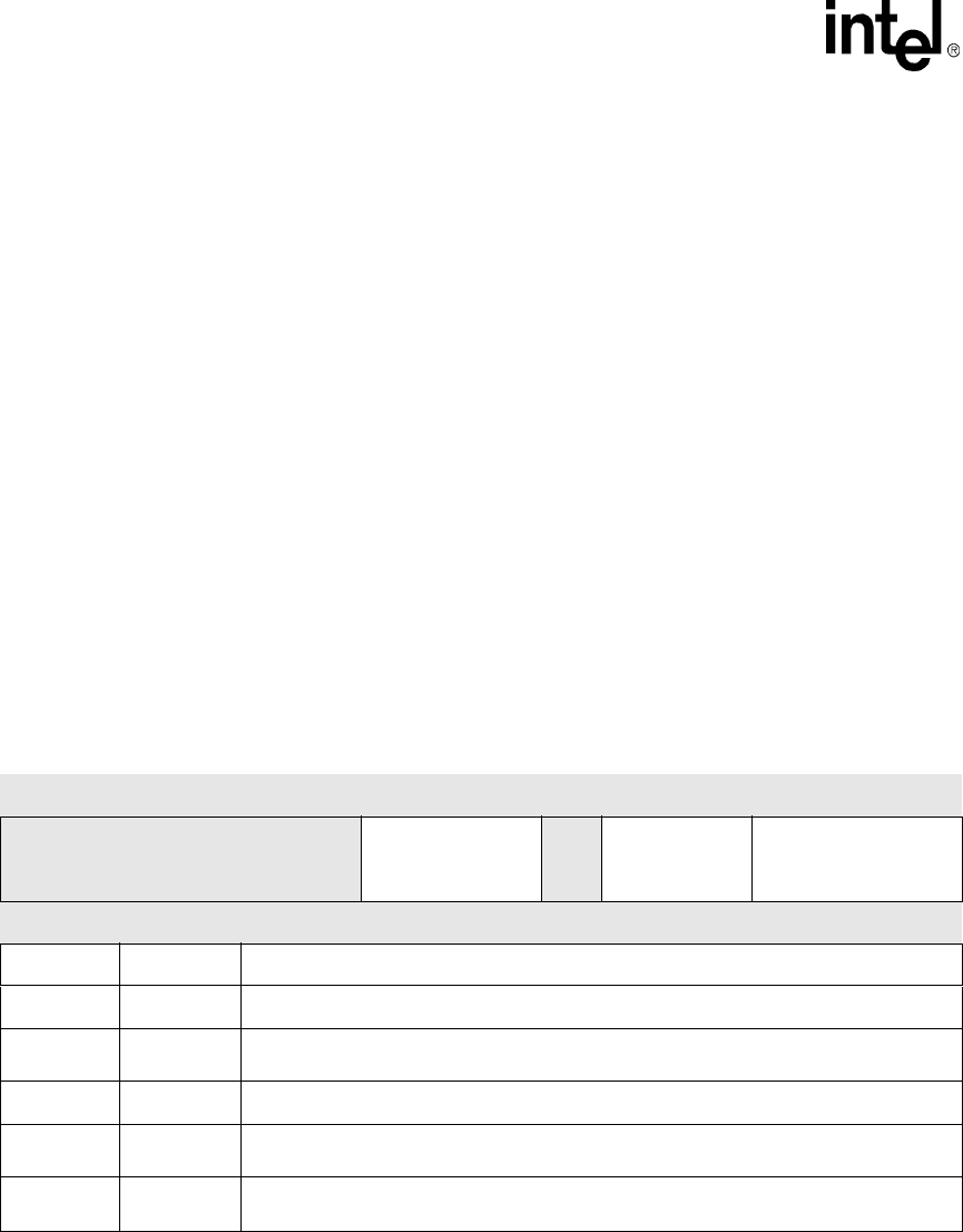
Table 6-26. MCMEM0/1 Bit Definitions
0x4800_0028
0x4800_002C
MCMEM0
MCMEM1
Memory Controller
Bit
31 30 29 28 27 26 25 24 23 22 21 20 19 18 17 16 15 14 13 12 11 10 9 8 7 6 5 4 3 2 1 0
reserved MEMx_HOLD
reserved
MEMx_ASST MEMx_SET
Reset
0 0 0 0 0 0 0 0 0 0 0 0 0 0 0 0 0 0 0 0 0 0 0 0 0 0 0 0 0 0 0 0
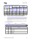
Bits Name Description
31:20 — reserved
19:14
MCMEMx_H
OLD
Minimum Number of memory clocks to set up address before command assertion for
MCMEM for socket x is equal to MCMEMx_HOLD + 2.
13:12 — reserved
11:7
MCMEMx_A
SST
Code for the command assertion time. See Table 6-29 for a description of this code and its
affects on the command assertion.
6:0
MCMEMx_S
ET
Minimum Number of memory clocks to set up address before command assertion for
MCMEM for socket x is equal to MCMEMx_SET + 2.