1-2 Intel® PXA255 Processor Developer’s Manual
Introduction
• DMA Controller
• LCD Controller
• AC97
• I
2
S
• MultiMediaCard
• FIR Communication
• Synchronous Serial Protocol Port
• I
2
C
• General Purpose I/O pins
• UARTs
• Real-Time Clock
• OS Timers
• Pulse Width Modulation
• Interrupt Control
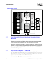
1.2.1 Memory Controller
The Memory Controller provides glueless control signals with programmable timing for a wide
assortment of memory-chip types and organizations. It supports up to four SDRAM partitions; six
static chip selects for SRAM, SSRAM, Flash, ROM, SROM, and companion chips; support for two
PCMCIA or Compact Flash slots
1.2.2 Clocks and Power Controllers
The processor functional blocks are driven by clocks that are derived from a 3.6864-MHz crystal
and an optional 32.768-kHz crystal.
The 3.6864-MHz crystal drives a core Phase Locked Loop (PLL) and a Peripheral PLL. The PLLs
produce selected clock frequencies to run particular functional blocks.
The 32.768-kHz crystal provides an optional clock source that must be selected after a hard reset.
This clock drives the Real Time Clock (RTC), Power Management Controller, and Interrupt
Controller. The 32.768-kHz crystal is on a separate power island to provide an active clock while
the processor is in sleep mode.
Power management controls the transition between the turbo/run, idle, and sleep operating modes.
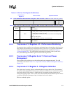
1.2.3 Universal Serial Bus (USB) Client
The USB Client Module is based on the Universal Serial Bus Specification, Revision 1.1. It
supports up to sixteen endpoints and it provides an internally generated 48-MHz clock. The USB
Device Controller provides FIFOs with DMA access to or from memory.


