


Intel® PXA255 Processor Developer’s Manual 10-21
UARTs
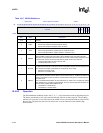
10.4.2.11 Scratchpad Register (SPR)
The SPR, shown in Table 10-16, has no effect on the UART. It is intended as a scratchpad register
for use by the programmer. It is included for 16550 compatibility.
This is a read/write register. Ignore reads from reserved bits. Write zeros to reserved bits.
10.4.3 FIFO Interrupt Mode Operation
This section describes how to service interrupts in FIFO mode.
10.4.3.1 Receive Interrupt
For a receive interrupt to occur, the receive FIFO and receive interrupts must be enabled. IIR[IID]
changes to show that receive data is available when the FIFO reaches its trigger level. IIR[IID]
changes to show the next waiting interrupt when the FIFO drops below the trigger level. A change
in IIR[IID] triggers an interrupt to the core. Software reads IIR[IID] to determine the cause of the
interrupt.
The receiver line status interrupt (IIR = 0xC6) has the highest priority and the received data
available interrupt (IIR = 0xC4) is lower. The line status interrupt occurs only when the character at
the front of the FIFO has errors.
The data ready bit (DR in the LSR) is set when a character is transferred from the shift register to
the Receive FIFO. The DR bit is cleared when the FIFO is empty.
10.4.3.2 Character Timeout Indication Interrupt
A character timeout indication interrupt occurs when the receive FIFO and character timeout
indication interrupt are enabled and all of the following conditions exist:
• At least one character is in the FIFO.
• The most recently received character was received more than four continuous character times
ago. If two stop bits are programmed, the second is included in this interval.
• The most recent FIFO read was performed more than four continuous character times ago.
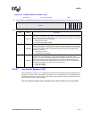
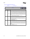
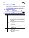
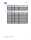
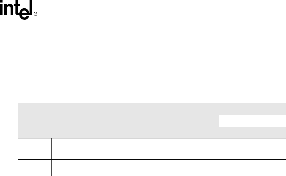
Table 10-16. SPR Bit Definitions
Base+0x1C Scratch Pad Register UART
Bit
31 30 29 28 27 26 25 24 23 22 21 20 19 18 17 16 15 14 13 12 11 10 9 8 7 6 5 4 3 2 1 0
reserved
SP
Reset 0 0 0 0 0 0 0 0 0 0 0 0 0 0 0 0 0 0 0 0 0 0 0 0 0 0 0 0 0 0 0 0
Bits Name Description
31:8 — reserved
7:0 SP
Scratch Pad
No effect on UART functionality