


Intel® PXA255 Processor Developer’s Manual 15-37
MultiMediaCard Controller
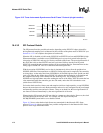
15.5.18 MMC_TXFIFO FIFO
MMC_TXFIFO, shown in Table 15-23, consists of two dual FIFOs, where each FIFO is eight bits
wide by 32 entries deep. This FIFO holds the data to be written to a card. It is a write only FIFO to
the software, and is written on boundaries eight bits wide. The eight bits of data are written on a 32-
bit APB and occupy the least significant byte lane (7:0).
This is a read/write register. Ignore reads from reserved bits. Write zeros to reserved bits.
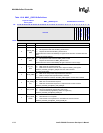
15.6 MultiMediaCard Controller Register Summary
Table 15-24 lists the address, name, and description of the MMC Controller Registers.
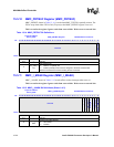
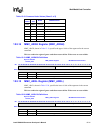
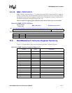
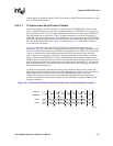
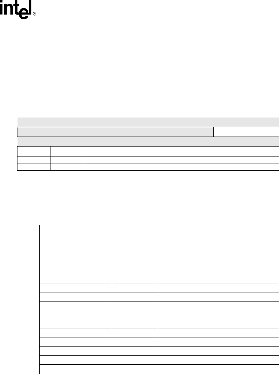
Table 15-23. MMC_TXFIFO, FIFO Entry
Physical Address
0x4110_0044
MMC_TXFIFO Entry MultiMediaCard Controller
Bit
31 30 29 28 27 26 25 24 23 22 21 20 19 18 17 16 15 14 13 12 11 10 9 8 7 6 5 4 3 2 1 0
reserved WRITE_DATA
Reset
0 0 0 0 0 0 0 0 0 0 0 0 0 0 0 0 0 0 0 0 0 0 0 0 x x x x x x x x
Bits Name Description
31:16 — reserved
7:0 WRITE_DATA One byte of write data
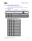
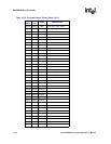
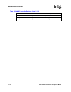
Table 15-24. MMC Controller Registers (Sheet 1 of 2)
Address Name Description
0x4110_0000 MMC_STRPCL Control to start and stop MMC clock
0x4110_0004 MMC_STAT MMC status register (read only)
0x4110_0008 MMC_CLKRT MMC clock rate
0x4110_000c MMC_SPI SPI mode control bits
0x4110_0010 MMC_CMDAT Command/response/data sequence control
0x4110_0014 MMC_RESTO Expected response time out
0x4110_0018 MMC_RDTO Expected data read time out
0x4110_001c MMC_BLKLEN Block length of data transaction
0x4110_0020 MMC_NOB Number of blocks, for block mode
0x4110_0024 MMC_PRTBUF Partial MMC_TXFIFO FIFO written
0x4110_0028 MMC_I_MASK Interrupt Mask
0x4110_002c MMC_I_REG Interrupt Register (read only)
0x4110_0030 MMC_CMD Index of current command
0x4110_0034 MMC_ARGH MSW part of the current command argument
0x4110_0038 MMC_ARGL LSW part of the current command argument