


Intel® PXA255 Processor Developer’s Manual 6-9
Memory Controller
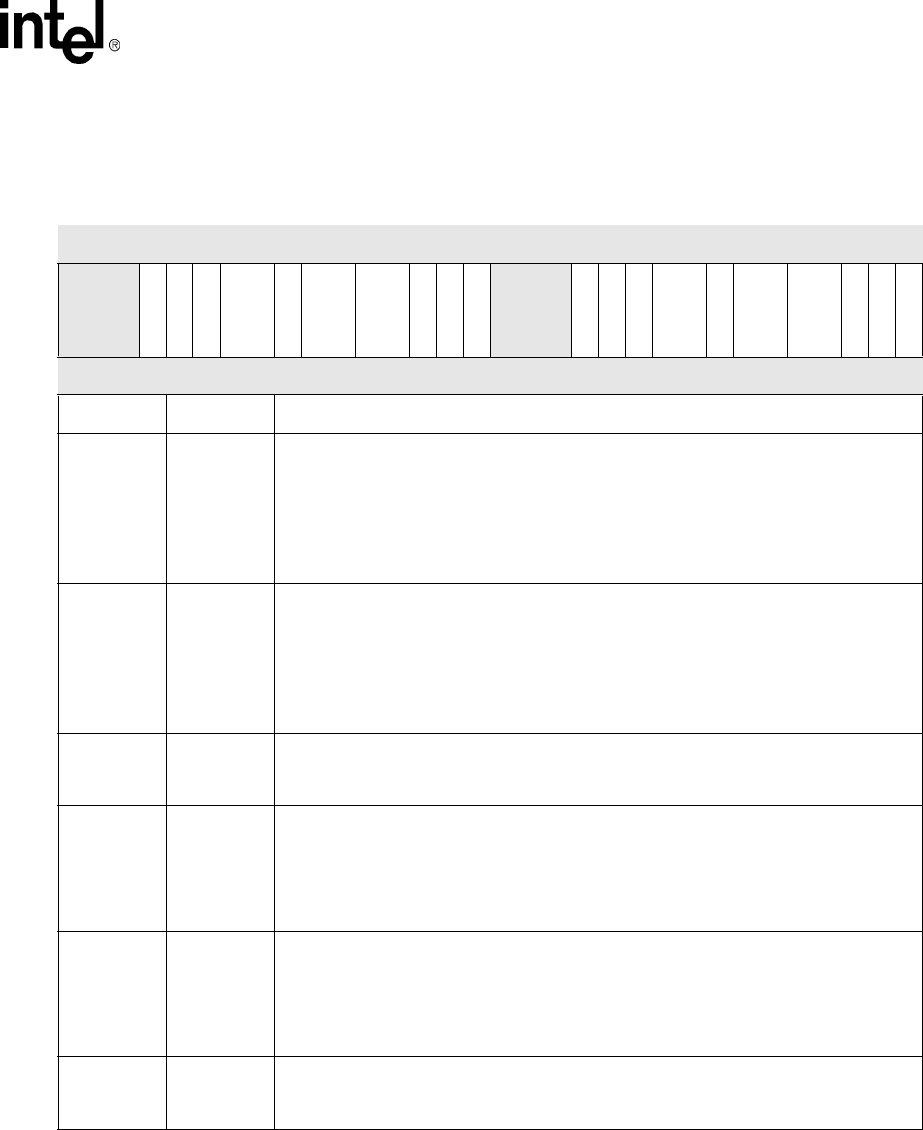
This is a read/write register. Ignore reads from reserved bits. Write zeros to reserved bits.
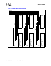
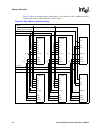
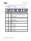
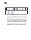
Table 6-2. MDCNFG Bit Definitions (Sheet 1 of 3)
0x4800_0000 MDCNFG Memory Controller
Bit
31 30 29 28 27 26 25 24 23 22 21 20 19 18 17 16 15 14 13 12 11 10 9 8 7 6 5 4 3 2 1 0
reserved
DSA1111_2
DLATCH2
DADDR2
DTC2
DNB2
DRAC2
DCAC2
DWID2
DE3
DE2
reserved
DSA1111_0
DLATCH0
DADDR0
DTC0
DNB0
DRAC0
DCAC0
DWID0
DE1
DE0
Reset 0 0 0 0 0 0 0 0 0 0 0 0 0 0 0 0 0 0 0 0 0 0 0 0 0 0 0 0 0 0 0 0
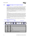
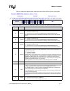
Bits Name Description
0DE0
SDRAM enable for partition 0
For each SDRAM partition, there is an enable bit. A single (non-burst) 32-bit (or 16-bit if
MDCNFG:DWID0=’1’) access (read or write) to a disabled SDRAM partition triggers a CBR
refresh cycle to all partitions. When all partitions are disabled, the refresh counter is
disabled.
0 – SDRAM partition disabled
1 – SDRAM partition enabled
1DE1
SDRAM enable for partition 1
For each SDRAM partition, there is an enable bit. A single (non-burst) 32-bit (or 16-bit if
MDCNFG:DWID0=’1’) access (read or write) to a disabled SDRAM partition triggers a CBR
refresh cycle to all partitions. When all partitions are disabled, the refresh counter is
disabled.
0 – SDRAM partition disabled
1 – SDRAM partition enabled
2DWID0
SDRAM data bus width for partition pair 0/1
0 – 32 bits
1 – 16 bits
4:3 DCAC0[1:0]
Number of Column Address bits for partition pair 0/1
00 - 8 column address bits
01 - 9 column address bits
10 - 10 column address bits
11 - 11 column address bits
6:5 DRAC0[1:0]
SDRAM row address bit count for partition pair 0/1
00 – 11 row address bits
01 – 12 row address bits
10 – 13 row address bits
11 – reserved
7DNB0
Number of banks in lower partition pair
0 – 2 internal SDRAM banks
1 – 4 internal SDRAM banks