


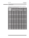
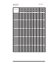
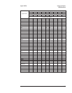
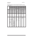

A10MHZ 10 MHz Clock — This is a 50% duty cycle, 10 MHz clock. This clock provides the timing for
the IIC processor on the A10 Rear Panel assembly.
ADCOLn ADC Overload — This line goes low when the input to the A5 Analog assembly’s ADC
exceeds its positive limit.
ADCULn ADC Underload — This line goes low when the input to the A5 Analog assembly’s ADC
exceeds its negative limit.
ADDATA Analog to Digital Data — This line is the digital representation of the input signal from the
A5 Analog assembly’s ADC controller. The ADC controller sends this digital representation to
the A6 Digital assembly once per sample (3.8147 ms).
B5MHZ 5 MHz Clock — This is a 50% duty cycle, 5 MHz clock. This clock provides the timing for
the GPIB controller on the A10 Rear Panel assembly.
BRESETn Buffered Reset — A low on this line resets the digital logic on the A5 Analog and A6 Digital
assembly. This line pulses low during power-up and power-down, and when the A7 CPU
assembly’s microprocessor executes the RESET instruction or is externally reset.
BTACH Buffered Tachometer — This line is a TTL representation of the A10 Rear Panel assembly’s
tachometer input.
CALP Calibration Signal — This line is the calibration signal from the A5 Analog assembly. During
calibration routines, this signal calibrates the input circuit on the A1 or A2 Input assembly. See
“Calibration Routine Description” in chapter 10, ‘’Internal Test Descriptions,’’ for further
details.
CEHPIBn GPIB Controller Chip Enable — This line is low whenever the GPIB controller is accessed for
read or write operations.
CEONIXn Chip Enable for the Parallel Port Controller — A low on this line enables the parallel port
controller on the A10 Rear Panel assembly.
CHSYNCn Channel Synchronize — A low on this line synchronizes the A5 Analog assembly’s ADC
controller with the A6 Digital assembly.
DACCLK Source Attenuation DAC Clock — This clock provides the timing for data transfer to the
A5 Analog assembly’s source attenuator and dc offset DAC. This clock is generated by the
A6 Digital assembly’s digital source.
DACDAT Source Attenuation DAC Data — This line provides the control for the A5 Analog assembly’s
attenuator DAC and dc offset DAC. This serial data line is generated by the A6 Digital
assembly’s digital source.
DACUPDn Source Attenuation DAC Latch — This is a control line from the A6 Digital assembly’s digital
source. A low on this line latches DACDAT after it is clocked into the A5 Analog assembly’s
attenuator DAC and dc offset DAC.
DITHER Dither — This line provides digital noise to the A6 Digital assembly’s digital filter. The noise
bandwidth is set by EFFSMP.
DSPTRIG DSP Trigger — This is a trigger line for the DSP processor on the A7 CPU assembly. The
DSP processor uses this line during gated measurements.
DSR Data Set Ready — Some devices connected to the serial port check this line for a high to verify
that the analyzer is connected and ready. The user can set this line high or set this line to go
high only when the analyzer is ready for data transfer.
ECLK E Clock — The gate arrays on the A6 Digital assembly use this clock for read and write timing.
EFFSMP Effective Sample Rate — This line sets the update rate for DITHER. The update rate is
frequency and span dependent, and controls the dither bandwidth.
Agilent 35670A Voltages and Signals
A99 Motherboard
9-29