


DIN Keyboard
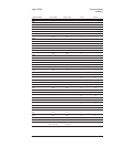
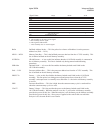
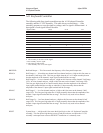
The following table lists signals at the DIN keyboard connector (A10 P200). A
description of each signal follows the table.
Signal Name
Pin
KEYCLK
1
KEYDAT
3
+5 V
4
Logic Gnd
2
Not Used
5
KEYCLK Key Board Clock — This clock synchronizes the transfer of keyboard data from the external
keyboard to the A10 Rear Panel assembly.
KEYDAT Key Board Data — This is 8-bit serial data from an external keyboard to the A10 Rear Panel
assembly .
Source Output
The source output is routed from P3 on the A5 Analog assembly through an SMB
cable to P201 on the A10 Rear Panel assembly. The A10 Rear Panel assembly then
routes the source signal to the Source BNC connector. In two channel analyzers, the
source output is also routed from P2 on the A5 Analog assembly through an SMB
cable to P11 on the A12 BNC assembly. The A12 BNC assembly then routes the
source signal to the Source BNC connector on the front panel. The source signal can
be random noise, burst random noise, periodic chirp, burst chirp, pink noise, or fixed
sine. The signal’s amplitude range is
±5 Vpk.
Tachometer Input
The A10 Rear Panel assembly converts the signal connected to the Tachometer BNC
connector to a TTL representation of the tachometer input (BTACH).
External Trigger Input
The A10 Rear Panel assembly buffers the signal connected to the External Trigger
BNC connector. The maximum trigger input level is ±25 Vpk. The minimum trigger
pulse width is 600 ns and the maximum trigger pulse rate is 800 kHz.
Agilent 35670A Voltages and Signals
A10 Rear Panel
9-17