


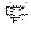
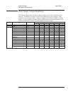

Gnd 1A, 2A, 7A, 7B, 7C, 8A,
14A, 14B, 14C, 21A,
24A, 24B, 24C, 25A,
30A, 31C
C2, A3, A8, A9, B9, C9,
A12, A19, B19, C19,
A25, A26, B26, C26,
A31, A32
••
Not Used
32B B1 — —
S This assembly is the source of the signal.
• This assembly uses the signal
⇔ This signal is bidirectional.
— This assembly does not use this signal.
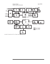
BD16 —31 Buffered Data Bus — This is the buffered processor data bus from the A7 CPU assembly. This
bus is further buffered on the A8 Memory assembly.
CPUSPCn CPU Space — This line goes low when the CPU space transfer occurs. When this line is low
the A8 Memory assembly does not respond.
DSACK0n —
DSACK1n
Data Strobe Acknowledge — During a write cycle, DSACK0n goes low after the A8 Memory
assembly places valid data on the data bus. During a read cycle, DSACK0n goes low after the
Memory assembly reads the data. When DSACK0n goes low and DSACK1n is low, 32 bits of
data are valid on PD0-15 and BD16-31. When DSACK0n goes low and DSACK1n is high, 8
bits of data are valid on BD24-31.
FLASHEN Flash Enable — This line is high only when the FLASH memory on the A8 Memory assembly
is being programmed. This line enables +12 V to the FLASH memory programming pin.
G20MHZ 20 MHz Clock — This is a 50% duty cycle, 20 MHz clock. This clock provides the timing for
the A8 Memory assembly.
MEMRESET Memory Reset — A high on this line resets the digital logic on the A8 Memory assembly. This
line pulses high during power-up and power-down, and when the A7 CPU assembly’s
microprocessor executes the RESET instruction or is externally reset.
PA0 — PA26 Processor Address Bus — This is the processor address bus from the A7 CPU assembly. This
bus is buffered on the A8 Memory assembly. PA0 and PA1 also operate with SIZE0 and
SIZE1 to specify the alignment of the operand.
PASn Processor Address Strobe — A low on this line starts a memory access cycle. This line pulses
low when a valid address is on the processor address bus (PA1 — PA23).
PD0 — 15 Processor Data Bus — This is the processor data bus from the A7 CPU assembly.
PRW Processor Read/Write — This line is high when the current memory cycle is a read and low
when the current memory cycle is a write.
SCL Serial Clock — This is the serial clock for the IIC bus. The IIC controller on the A7 CPU
assembly generates this clock to synchronize the transfer of data on the IIC bus.
SDA Serial Data — This is the IIC bus bidirectional data line. This line transmits real-time clock
data between the A7 CPU assembly and the A8 Memory assembly in 8-bit frames. The IIC
controller on the CPU assembly controls data transfers on the IIC bus.
Voltages and Signals Agilent 35670A
A8 Memory
9-10