


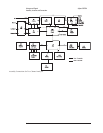
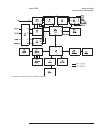
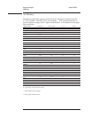
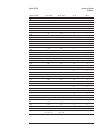
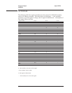
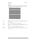

A9 NVRAM
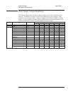
The following table lists signals routed between the optional A9 NVRAM assembly
and the A8 Memory assembly. This table shows several things — if the assembly
generates or uses the signal or voltage, and if a signal is bidirectional. A description of
each signal follows the table.
Signal Name
Pin(s) A8 P2 A9 J1
BASn
A6 • •
MD24 B4
⇔⇔
MD25 C4
⇔⇔
MD26 B3
⇔⇔
MD27 C3
⇔⇔
MD28 B2
⇔⇔
MD29 C2
⇔⇔
MD30 B1
⇔⇔
MD31 C1
⇔⇔
NVPRESn
A16 — S
OPRAMn
A2 S •
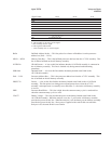
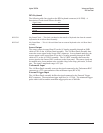
PA0
C6 S •
PA1
B6 S •
PA2
C7 S •
PA3
B7 S •
PA4
C8 S •
PA5
B8 S •
PA6
C9 S •
PA7
B9 S •
PA8
C10 S •
PA9
B10 S •
PA10
C12 S •
PA11
B12 S •
PA12
C13 S •
PA13
B13 S •
PA14
C14 S •
PA15
B14 S •
PA16
C15 S •
PA17
B15 S •
S This assembly is the source of the signal.
• This assembly uses the signal.
⇔ This signal is bidirectional.
— This assembly does not use this signal.
Voltages and Signals Agilent 35670A
A9 NVRAM
9-12