


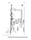
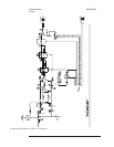
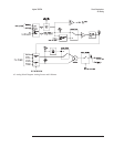
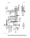

ADC Input Switch Connects the first pass signal to the low pass filter on the first pass. On the second pass, the
ADC Input Switch connects the second pass signal to the low pass filter. After the second pass,
the ADC Input Switch connects a 0.34 Vdc signal to the low pass filter to reset the 8-Bit ADC.
Low Pass Filter Reduces noise and prevents high frequency signals from overdriving the 8-bit ADC.
8-Bit ADC Converts the signal to an 8-bit word.
2nd Pass DAC Converts the first pass word plus dither to a voltage that is sent to the 2nd Pass Circuit.
2nd Pass Circuit Compares the output of the 2nd Pass DAC (converted first pass signal plus dither) to the
original input signal (which is still held by the Track & Hold) and produces a difference
voltage. This difference voltage is the second pass signal.
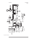
±6.2 Voltage Reference Reduces the error due to temperature variations. This voltage reference is used by the 1st Pass
Circuit, 2nd Pass Circuit, ADC Input Switch, 8-bit ADC, and Track & Hold. Since the 8-bit
ADC’s gain is derived from this voltage reference, the adjustment for this voltage reference is
also the gain adjustment for the 8-bit ADC.
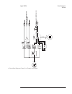
Trigger-Level Input Connects the appropriate signal to the Trigger-Level Comparator.
Temperature Sensor Senses the analyzer’s internal temperature. If the internal temperature exceeds a set point, this
circuit sets FANTRIP high which turns the fan back on if the fan was turned off by the user. If
the temperature becomes excessive, this circuit sets SHUTn low which forces all A98 Power
Supply assembly output voltages to zero.
Trigger-Level
Comparator
Compares the signal level with the value from the Trigger Level DAC.
Trigger Level DAC Provides the trigger level. The A7 CPU assembly sets the trigger level via the IIC bus using
the value set with the [ TRIGGER SETUP ] and [ LEVEL ] softkeys.
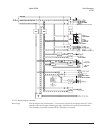
Mic Buffer Buffers control signals for the optional sound intensity probe. When a measurement is being
made, the MEAS line goes high to turn on the probe’s green LED. If an overload occurs
during the measurement, the OVLD line goes high to turn on the probe’s yellow LED.
IIC Interface Provides the interface between the A7 CPU assembly and the A5 Analog assembly.
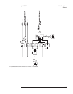
Serial In Parallel Out
Shift Register
Provides the mode control to the Analog Switches and the digital source data to the DAC.
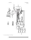
Signal DAC Converts the digital source data to an analog signal. During calibration, the analog signal from
the DAC is buffered or attenuated by 10. The calibration signal (CALP) is then routed to each
input channel.
Programmable Low-Pass
Filter
Filters the analog signal from the Signal DAC when selected. Filter bandwidth is set by
LPFCLK from the A6 Digital assembly; it can be set from 51.2 kHz to 1.56 Hz in binary steps.
Random noise and burst random noise signals below 51.2 kHz are filtered. Arbitrary signals
below 51.2 kHz can be filtered using the front panel keys.
100 kHz Low-Pass
Filter
Provides image rejection, reduces noise, and prevents high frequency signals from overdriving
the Attenuator DAC. It also compensates for sinx/x rolloff at the 262.144 kHz sample rate.
Attenuator DAC/DC
Offset DAC
Attenuates the signal and generates a dc offset.
Pink Noise Filter Shapes the noise for a flat response in octave mode.
Summing Combines the signal with the dc offset.
Output Amplifier Amplifies and buffers the signal. A relay disconnects the signal from the SOURCE connector
10 ms before the A98 Power Supply assembly’s output voltages fall out of regulation.
Circuit Descriptions Agilent 35670A
A5 Analog
8-20