


Agilent N5161A/62A/81A/82A/83A MXG Signal Generators User’s Guide 19
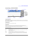
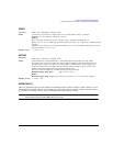
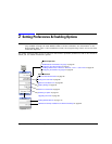
Preliminary Signal Generator Overview
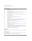
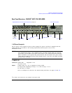
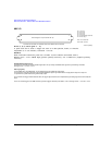
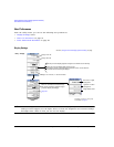
Preliminary Rear Panel Overview – N5161A/62A
1
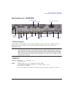
/81A/82A MXG
EVENT 1
PAT TRIG
DIGITAL BUS I/O
This is a proprietary bus used by Agilent Technologies signal creation software. This connector is not
operational for general purpose use. Signals are present only when a signal creation software option
is installed (for details, refer to http://www.agilent.com/find/signalcreation).
NOTE The MXG’s Digital BUS I/O connector can be used for enabling operation with the Agilent
Technologies N5106A PXB MIMO Receiver Tester.
Connector
female BNC Impedance: nominally 50
Ω
Signal A pulse that can be used to trigger the start of a data pattern, frame, or timeslot.
Adjustable to ± one timeslot; resolution = one bit
Markers
Each Arb–based waveform point has a marker on/off condition associated with it.
Marker 1 level = +3.3 V CMOS high (positive polarity selected); –3.3 V CMOS low (negative polarity
selected).
Output on this connector occurs whenever Marker 1 is on in an Arb–based waveform (see “Using
Waveform Markers” on page 147).
Damage Levels < −4 and > +8 V
Connector
female BNC Impedance: nominally 50
Ω
Signal A TTL/CMOS low to TTL/CMOS high, or TTL/CMOS high to TTL/CMOS low edge trigger.
The input to this connector triggers the internal digital modulation pattern generator to start
a single pattern output or to stop and re–synchronize a pattern that is being continuously
output. To synchronize the trigger with the data bit clock, the trigger edge is latched, then
sampled during the falling edge of the internal data bit clock.
This is the external trigger for all ARB waveform generator triggers.
Minimum Trigger Input Pulse
Width
(high or low) = 100 ns
Minimum Trigger Delay (trigger edge to first bit of frame) = 1.5 to 2.5 bit clock periods
Damage Levels < −4 and > +8 V