


18 Agilent N5161A/62A/81A/82A/83A MXG Signal Generators User’s Guide
Signal Generator Overview Preliminary
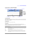
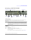
Rear Panel Overview – N5161A/62A
1
/81A/82A MXG Preliminar
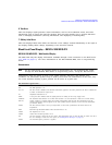
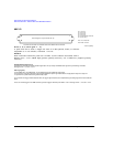
Digital Modulation Connectors (Vector Models Only)
I OUT, Q OUT, OUT, OUT
EXT CLK
Connector Type: female BNC Impedance: 50 Ω
DC–coupled
Signal
I OUT The analog, in–phase component of I/Q modulation from the internal baseband generator.
Q OUT The analog, quadrature–phase component of I/Q modulation from the internal baseband
generator.
OUT
Used in conjunction with the I OUT connector to provide a balanced
a
baseband stimulus.
a
Balanced signals are signals present in two separate conductors that are symmetrical relative to ground, and are opposite in polarity
(180 degrees out of phase).
OUT
Used in conjunction with the Q OUT connector to provide a balanced
a
baseband stimulus.
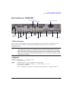
Damage Levels > 1 Vrms DC Origin Offset typically <10 mV
Output Signal Levels into a 50 Ω Load
• 0.5 V
pk
, typical, corresponds to one unit length of the I/Q vector
• 0.69 V
pk
(2.84 dB), typical, maximum crest factor for peaks for π/4 DQPSK, alpha = 0.5
• 0.71 V
pk
(3.08 dB), typical, maximum crest factor for peaks for π/4 DQPSK, alpha = 0.35
• Typically 1 V
p–p
maximum
Connector female BNC Impedance nominally 50 Ω
Signal An externally supplied TTL or CMOS bit clock signal where the rising edge aligns with the
beginning data bit.
The falling edge is used to clock external signals.
This signal is used with digital modulation applications.
Damage Levels < −4 and > +8 V Maximum Clock Rate 50 MHz
I
Q
I
Q