


AWG2005 Service Manual
3Ć1
Theory of Operation
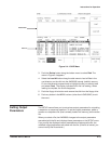
This section describes the basic operation of the major circuit blocks or
modules in the AWG2005. Section 9, Diagrams, includes two block diaĆ
grams and an interconnect diagram. Figure 9Ć1 shows the modules and
functional blocks of the AWG2005 with Option 02, 04, 05 and 09 installed.
Figure 9Ć2 shows how the modules interconnect.
The module overview describes the basic operation of each functional circuit
block.
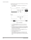
The AWG2005 Arbitrary Waveform Generator is a portable, twoĆ or fourĆ
channel instrument. For each channel, the AWG2005 reads the digital waveĆ
form data loaded into its waveform memory. The point rate clock determines
the rate at which the data is read. The AWG2005 converts the data from
digital to analog format and outputs the resulting arbitrary waveform.
Clock Oscillator (A1 Clock Board)
The clock circuit is a PLL oscillator that uses a 12.8 MHz reference crystal. It
supplies a point rate clock that is adjustable from 20 MHz to 0.01 Hz for
reading data from channel waveform memory.
When an external clock source is selected, the external clock signal is
passed directly through to the Clock board and used for reading waveform
data in memory.
Clock Sweep Oscillator (A31 Clock Sweep Board)
In addition to the description for the Clock Sweep Oscillator, it provides the
clock sweep from 20 MHz to 0.03 Hz.
Sequencer (A2 AWG Board)
This sequencer block controls the waveform memory addresses read out
according to the contents of a sequence file.
Waveform Memory (A2 AWG Board)
This functional block contains the memory that holds the waveform digital
data. There are 12 bits for waveform data and one bit for waveform markers
(for each channel).
Module Overview