


Options and Accessories
AWG2005 Service Manual
7Ć3
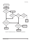
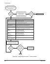
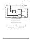
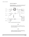
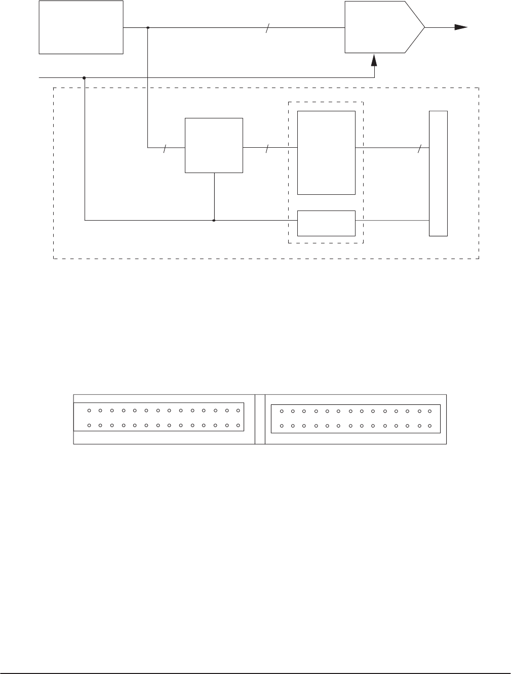
Option 04
Output
Connector
Clock
Data
Buffer
Waveform
Memory
D / A
Latch
D0
~
D11
CLOCK
12
12
Clock
Data
12 Bits
12
12
Figure 7Ć1:ăOption 04 Block Diagram
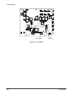
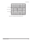
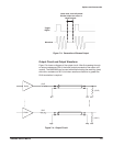
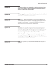
Output Connector Configuration
Figure 7Ć2 shows the shape of the output connector and its pin locations.
Table 7Ć2 lists the output signal for each pin.
1
2
25
26
1
2
25
26
CH1 DIGITAL DATA OUT
CH2 DIGITAL DATA OUT
Figure 7Ć2:ăOption 04 Output Connector