


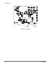

Options and Accessories
Options
7Ć4
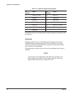
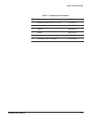
TableĂ7Ć2:ăOption 04 Digital Output Signals
Pin
Number
Signal Pin
Number
Signal
1 Data bit 0 (LSB) 15 Data bit 7
3 Data bit 1 17 Data bit 8
5 Data bit 2 19 Data bit 9
7 Data bit 3 21 Data bit 10
9 Data bit 4 23 Data bit 11 (MSB)
11 Data bit 5 24 Clock
13 Data bit 6
Pins other than above are connected to ground. The pin assignments are identical for both
CH1 and CH2.
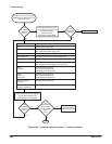
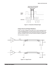
Operation
Basically, operations are in correspondence with analog output for the
AWG2005 arbitrary waveform generator. When a waveform is not being
output, the waveform's initial data may be output to the connector. At this
time, the clock is not generated.
When starting the waveform output, the clock is generated and the data is
updated.
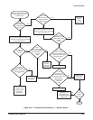
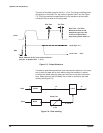
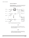
NOTE
Excess output can be generated in the data clock (see Figure 7Ć3)
when loading a new waveform into waveform memory, when resetĆ
ting the waveform memory, or during the hold off.