


Hardware Initialization States
3-19
Peripheral Functions
3.5 Hardware Initialization States
The RESET pin is configured at all times as an external interrupt. It provides
for a hardware initialization of the C614. When the RESET pin is held low, the
device assumes a deep sleep state and various control registers are
initialized. After the RESET pin is taken high once again, the Program Counter
is loaded with the value stored in the RESET Interrupt Vector.
Note: Internal Power Reset Function
There is no power-on reset function internal to the C614. After the initial pow-
er-up or after an interruption in power, the RESET pin must be cycled low-to-
high. The application circuitry must therefore provide a mechanism for ac-
complishing this during a power-up transition or after a power fluctuation.
The application circuits shown in Section 6.1,
Application Circuits
, illustrate
one implementation of a reset-on-power-up circuit. The circuit consists of an
RC network (100 kΩ, 1 µF). When powering V
DD
from 0 V to 4.5 V, the circuit
provides some delay on the RESET pin’s low-to-high transition. This delay
helps to ensure that the C614 initialization occurs
after
the power supply has
had time to stabilize between V
DD
MIN and V
DD
MAX. V
DD
MIN and V
DD
MAX
are the minimum and maximum supply voltages as rated for the device. The
circuit shown, however, may not shield the RESET pin from
every
kind of rapid
fluctuation in the power supply. At any time that the power supply falls below
V
DD
MIN, even momentarily, then the RESET pin must be held low and then
high once again, either by the user of the device or by some other external cir-
cuitry. Refer to Chapter 8,
MSP50C614 Electrical Specifications
, for a charac-
terization of the values V
DD
MIN, V
DD
MAX, V
IL
, and V
OL
. (V
IL
and V
OL
are the
low-level and high-level input voltages, respectively, which dictate the precise
levels of transition for RESET.)
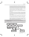
When the RESET pin is held low, the C614 is considered reset and has the
following internal states:
RESET low . . .
I/O ports are be placed in a high impedance Input condition: Ports A, B,
C, D, and E.
All outputs on Port G is are set to low (0x0000).
Device is placed in a deep sleep state (refer to reduced power mode IV
in Table 2–7).
PLL circuitry, master clock, CPU clock, and TIMERs are stopped.
Current draw from the V
DD
is less than 10 µA in this condition.
Interrupt flag register (IFR at address 0x39) is
not
automatically cleared.
Internal RAM is
not
automatically cleared.