Execution Timing
2-33
MSP50C614 Architecture
However, the general specification of the adjustment can be useful in certain
circumstances. For example, the adjustment can be used to obtain a program-
matic increase or decrease in the speed of the RTO reference. The default val-
ue for the adjustment, after RESET low, is all zeros. The zero value generates
the slowest programmable rate for the RTO reference. The maximum value,
0x3F, generates the fastest programmable rate for the RTO reference. The full
range from 0x00 to 0x3F, effects an approximate +62% change (based on the
RTO resistor value specification). The change is nonlinear and nonlinear it
changes from one device to another.
On the P614 part, the above method does not cause in the correct trim value
to be loaded in ClkSpdCtrl. MSP50P614 is an EPROM device. Any
preprogrammed value is erased when the chip goes through a UV erase
procedure. The RTO trim value must, therefore, be computed separately for
each chip. RTO trim values differ from one chip to another, is identical for the
same chip.
Note: Register Trim Value
A resistor trim value is only needed when the resistor trimmed oscillator
(RTO) is used. The MSP50P614 device must determine the trim value sepa-
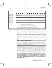
rately and use this value in the ClkSpdCtrl register bits 15–11 and 9, but C614
device needs to copy bit 0 of I/O location 0x2F to bit 9 of the ClkSpdCtrl regis-
ter and bits 5 through 1 to bits 15 through 11 of ClkSpdCtrl register.
This software-controlled trim for the RTO is not a replacement for the external
reference-resistor mounted at pins OSC
IN
and OSC
OUT
. Also, note that this
adjustment has no effect on the rate of the CRO reference oscillator.
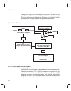
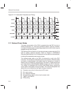
2.10 Execution Timing
For executing program code, the C614’s core processor has a three-level
pipeline. The pipeline consists of instruction fetch, instruction decode, and
instruction execution. A single instruction cycle is limited to one program Fetch
plus one data memory read or write. The master clock consists of two phases
with non-overlap protection. A fully static implementation eliminates pre-
charge time on busses or in memory blocks. This design also results in a very
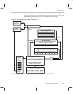
low power dissipation. Figure 2–9 illustrates the basic timing relationship
between the master clock and the execution pipeline.


