


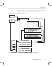
Memory Organization: RAM and ROM
2-18
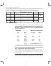
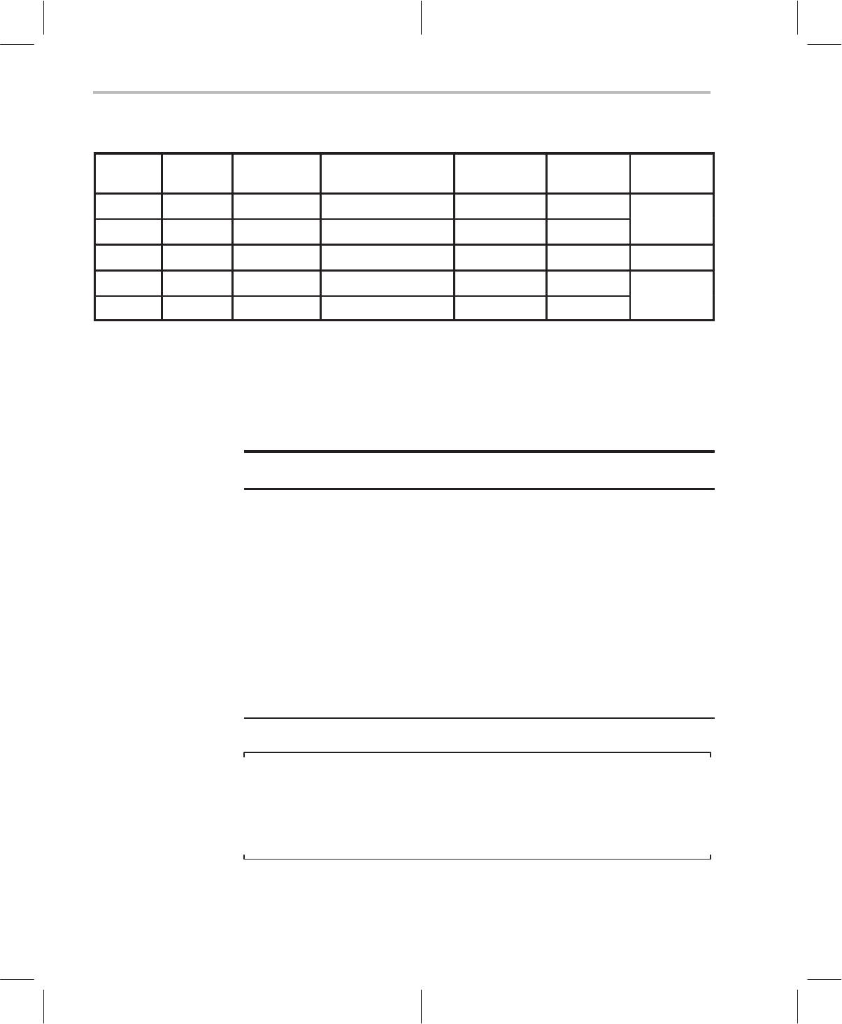
Table 2–2. Summary of C614’s Peripheral Communications Ports (Continued)
I/O Map
Address
Width of
Location
Allowable
Access
Control Register Name Abbreviation
State after
RESET LOW
Section for
Reference
0x3A 16 bits read & write TIMER1 period PRD1 0x0000
28
0x3B 16 bits read & write TIMER1 count-down TIM1 0x0000
2
.
8
0x3D 16 bits WRITE only Clock speed control ClkSpdCtrl 0x0000 2.9.3
0x3E 16 bits read & write TIMER2 period PRD2 0x0000
28
0x3F 16 bits read & write TIMER2 count-down TIM2 0x0000
2
.
8
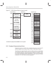
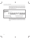
2.6.3 Interrupt Vectors
When its event has triggered and its service has been enabled, an interrupt
causes the program counter to branch to a specific location. The destination
location is stored (programmed) in the interrupt vector, which resides in an up-
per address of ROM. The following table lists the ROM address associated
with each interrupt vector:
Interrupt Name
ROM address of
Vector
Event Source Interrupt Priority
INT0 0x7FF0 DAC Timer Highest
INT1 0x7FF1 TIMER1 2nd
INT2 0x7FF2 TIMER2 3rd
INT3 0x7FF3 port D
2
4th
INT4 0x7FF4 port D
3
5th
INT5 0x7FF5 all port F 6th
INT6 0x7FF6 port D
4
7th
INT7 0x7FF7 port D
5
Lowest
0x7FFE storage for ROM Protection Word
RESET
0x7FFF storage for initialization vector
Note: ROM Locations that Hold Interrupt Vectors
ROM locations that hold interrupt vectors are reserved specifically for this
purpose. Additional ROM locations 0x7FF8 - 0x7FFD are reserved for future
expansion. Like the interrupt vectors, they should not be used for general
program storage.
The branch to the program location that is specified in the interrupt vector is,
of course, contingent on the occurrence of the trigger event. Refer to Section