


Clock Control
2-31
MSP50C614 Architecture
Note: ClkSpdCtrl Bits 8 and 9
When bit 8 is set in the ClkSpdCtrl register, the crystal oscillator bit (bit 9) be-
comes the least significant bit of the 6-bit resistor trim value. Thus, bits 15–11
and 9 make up the 6-bit resistor trim value. For example, if the ClkSpdCtrl
register is 00010X11XXXXXXXX (X means don’t care, bold numbers are re-
sistor trim bits), then the resistor trim value is equal to five.
The default value of the ClkSpdCtrl is 0x0000, which means that neither option
is enabled by default. Immediately after a RESET LOW-to-HIGH, and
regardless of whether a resistor or a crystal is installed across OSC
IN
/
OSC
OUT
, the C614 does not have a reference oscillator running. In the
absence of a reference, however, the PLL still oscillates; it bottoms-out at a
minimum frequency. The master clock, in turn, runs at a very slow frequency
(less than 100 kHz) in the absence of a reference oscillator. Under this
condition, program execution is supported at a slow rate until one of the two
references (RTO or CRO) is enabled in software. (Refer to Chapter 8,
MSP50C614 Electrical Specifications
, for a more precise characterization of
the master clock rate under these conditions.)
Once a reference oscillator has been enabled, the speed of the master clock
(MC) can be set and adjusted, as desired. Bits 7 through 0 in the ClkSpdCtrl
constitute the PLL multiplier (PLLM). The value written to the PLLM controls
the effective scaling of the MC, relative to the 131.07 kHz base frequency. A
0 value in PLLM yields the minimum multiplication of 1, and a 255 value in
PLLM yields the maximum multiplication of 256. The resulting MC frequency,
therefore, is controlled as follows:
MC Master clock frequency kHz = (PLLM register value + 1) × 131.07 kHz
CPU Clock frequency kHz = (PLLM register value + 1) × 65.536 kHz
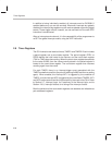
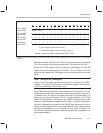
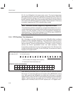
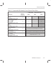
The configuration of bits in the clock speed control register appears below:
ClkSpdCtrl register
address 0x3D (16-bit wide location)
WRITE only 15 14 13 12 11 10 09 08 07 06 05 04 03 02 01 00
T5 T4 T3 T2 T1 I C or T0 R MMMMMMMM
T : RTO oscillator-Trim adjust R : enable Resistor-trimmed oscillator
I : Idle State clock Control M : PLLM multiplier bits for MC
C : enable Crystal oscillator
(or T0 if R is set
0x0000 : default state after RESET LOW