


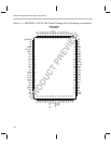
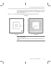
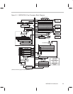

Terminal Assignments and Signal Descriptions
1-10
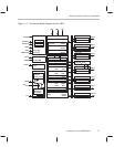
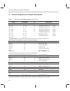
1.6 Terminal Assignments and Signal Descriptions
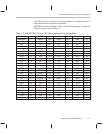
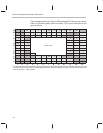
Table 1–1. Signal and Pad Descriptions for the C614
SIGNAL PAD NUMBER I/O DESCRIPTION
Input/Output Ports
PA
0
– PA
7
75 → 68 I/O Port A general-purpose I/O (1 Byte)
PB
0
– PB
7
85 → 78 I/O Port B general-purpose I/O (1 Byte)
PC
0
– PC
7
8 → 1 I/O Port C general-purpose I/O (1 Byte)
PD
0
– PD
7
18 → 11 I/O Port D general-purpose I/O (1 Byte)
PE
0
– PE
7
63 → 56 I/O Port E general-purpose I/O (1 Byte)
PF
0
– PF
7
31 → 24 I Port F key-scan input (1 Byte)
PG
0
– PG
7
49 → 42
O Port G dedicated output (2 Bytes)
PG
8
– PG
15
39 → 32
Pins PD
4
and PD
5
may be dedicated to the comparator function, if the comparator enable bit is set.
Refer to Section 3.3,
Comparator
, for details. (Currently not supported)
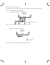
Scan Port Control Signals
SCANIN 54 I Scan port data input
SCANOUT 50 O Scan port data output
SCANCLK 53 I Scan port clock
SYNC 52 I Scan port synchronization
TEST
PGMPULSE
51 I C614 : test modes
P614 : programming pulse
The scan port pins must be bonded out on any C614 production board.
Consult the “Important Note regarding Scan Port Bond Out”, Section 7.1.1,
Scan Port Bond Out
.
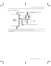
Oscillator Reference Signals
OSC
IN
65 I Resistor/crystal reference in
OSC
OUT
66 O Resistor/crystal reference out
PLL 67 O Phase-lock-loop filter
DAC Sound Output
DAC
P
22 O Digital-to-analog output 1 (+)
DAC
M
20 O Digital-to-analog output 2 (–)
Initialization
RESET 55 I Initialization
Power Signals
V
SS
9, 19
†
, 40, 64, 76 Ground
V
DD
10, 21
†
, 23, 41, 77 Processor power (+)
†
Pads V
SS
(19) and V
DD
(21) service the DAC circuitry. Their pins tend to sustain a higher current draw. A dedicated decoupling
capacitor across these pins is therefore required. Refer to Section 6.1,
Application Circuits
, for details.