2-4
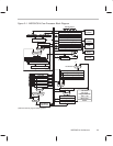
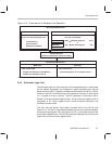
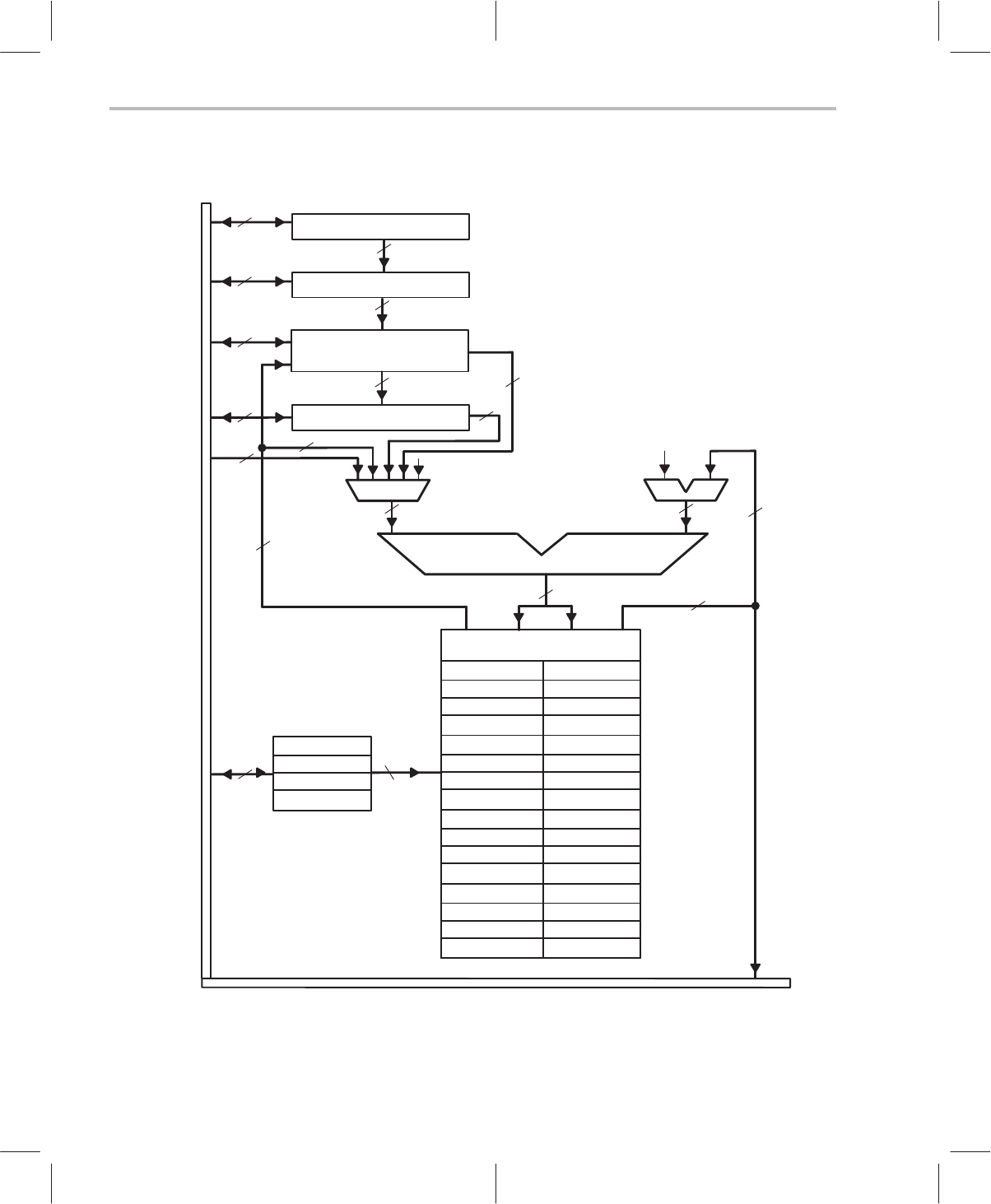
Figure 2–2. Computational Unit Block Diagram (The shaded boxes represent internal
programmable registers.)
Accumulators
5
16
AC3
AC2
AC1
AC0
Read/Write
AC7
AC6
AC5
AC4
AC11
AC10
AC9
AC8
AC15
AC14
AC13
AC12
AC19
AC18
AC17
AC16
AC23
AC22
AC21
AC20
AC27
AC26
AC25
AC24
AC31
AC30
AC29
AC28
AP3
AP2
AP1
AP0
5
Internal Databus – 16 bit
Shift Value (SV)
Multiplier Register (MR)
17 bit x 17 bit
Multiplexer
Product High (PH)
16
16
16 MSB
16
16
16
16
16
16
0
16
(Product Low, PL)
16 LSB
16
ALU
AB
16
0
16


