


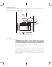
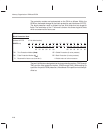
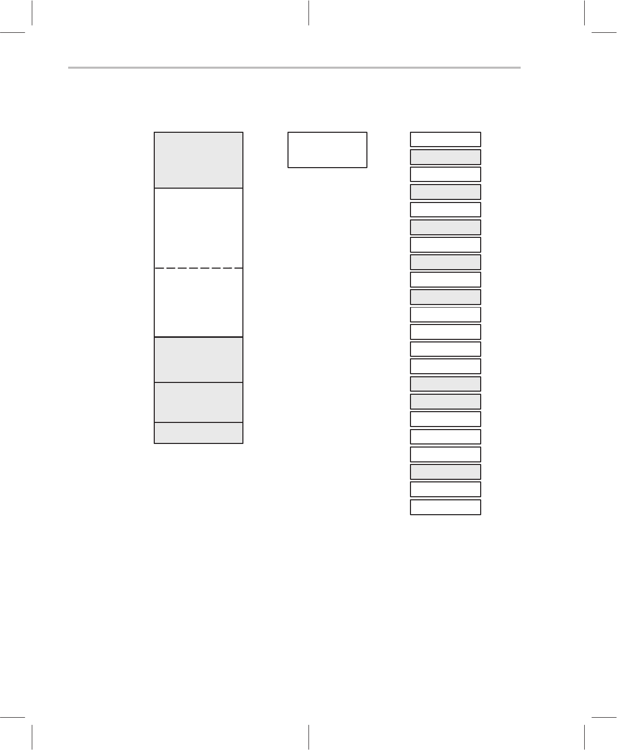
Memory Organization: RAM and ROM
2-16
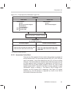
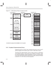
Figure 2–7. C614 Memory Map (not drawn to scale)
0x00
Program Memory
0x0000
Internal Test Code
2048 x 17 bit
0x07FF
0x0800
0x7F00
0x7FF0
0x7FF7
(reserved)
User ROM
30704 x 17 bit
(C614 : read-only)
(P614 : EPROM)
Usable Interrupt
Vectors†
8 x 17 bit
Macro Call Vectors
255 x 17 bit
(overlaps interrupt
vector locations)
0x0000
RAM
640 x 17 bit
Data Memory
0x027F
Peripheral Ports
PA
0–7
data
0x04
PA
0–7
ctrl
0x08 PB
0–7
data
0x0C
PB
0–7
ctrl
0x10
PC
0–7
data
0x14
PC
0–7
ctrl
0x18
PD
0–7
data
0x1C
PD
0–7
ctrl
0x20
PE
0–7
data
0x24
PE
0–7
ctrl
0x28
PF
0–7
data
0x2C
PG
0–15
data
0x30
DAC data
0x34
DAC ctrl
0x38 IntGenCtrl
0x39
IFR
0x3A
PRD1
0x3B
TIM1
0x3D
ClkSpdCtrl
0x3E
PRD2
0x3F
TIM2
0x2F
RTRIM
Unusable Interrupt
Vectors
(reserved)
RESET vector
0x7FF8
0x7FFE
0x7FFF
Shaded boxes highlight dedicated ROM and control registers.
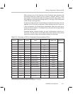
2.6.2 Peripheral Communications (Ports)
Peripheral functions in the C614 are controlled using one or more of the I/O
address-mapped communications ports. Table 2–2 describes the ports.
The width of each mapped location, shown in width of location, is independent
of the address spacing. In other words, some registers are smaller in width
than the spacing between neighboring addresses. The few unused bits appear
to the right of the LSB values within the DAC Data register, address 0x30 (refer
to Section 3.2.2,
DAC Control and Data Registers
).