


Application Circuits
6-3
Applications
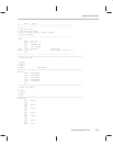
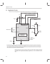
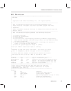
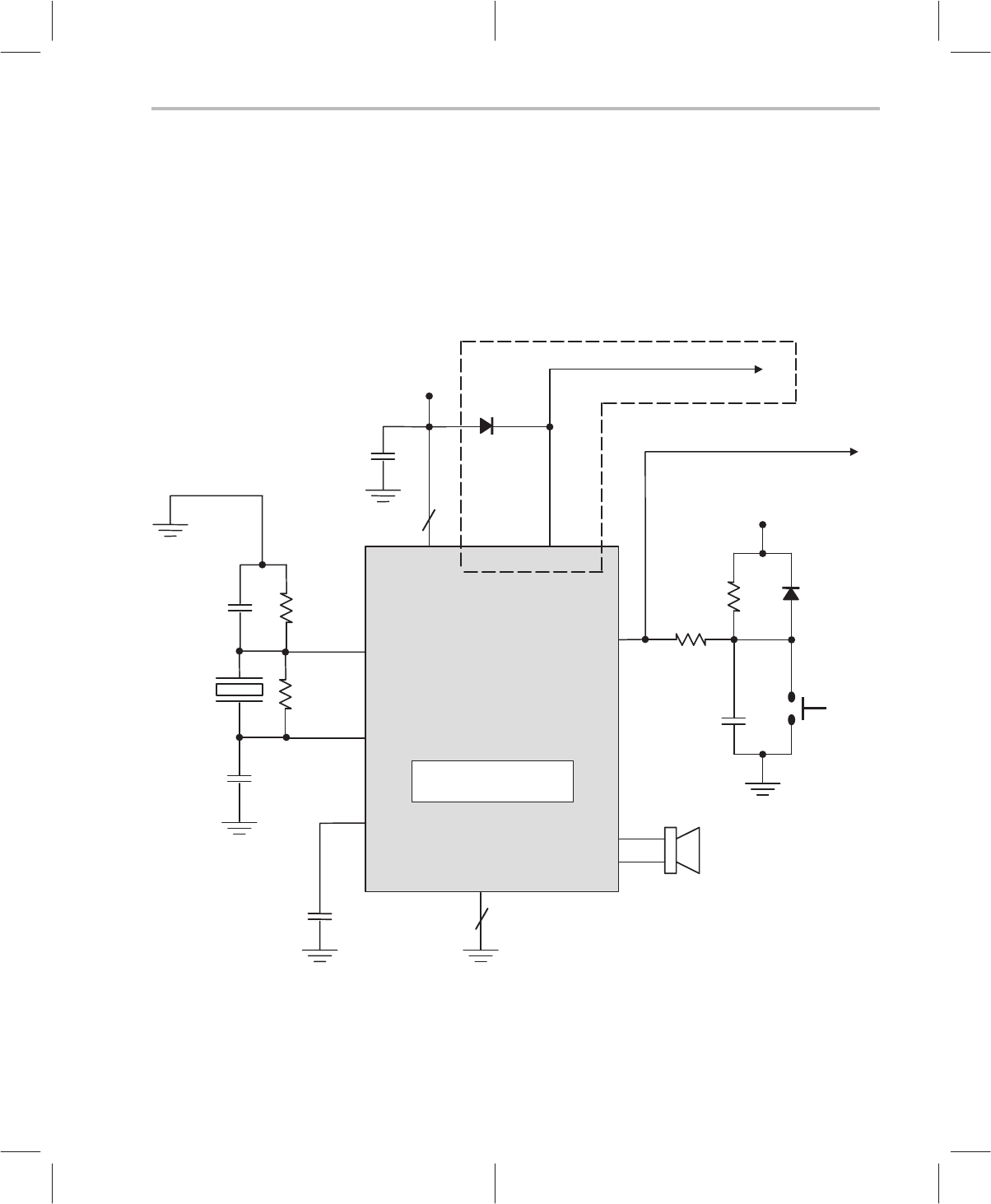
It is of particular importance to provide a separate decoupling capacitor for the
V
DD
, V
SS
pair which services the DAC. These pins are pad numbers 21 and
19, respectively. The relatively high current demands of the digital-to-analog
circuitry make this a requirement.
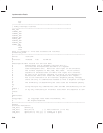
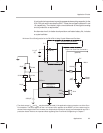
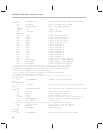
An alternate circuit, for better clock-precision and better battery life, includes
a crystal oscillator:
†
The diode across V
DD
and V
PP
may be omitted (shorted), if the application does not require use of the Scan
Port Interface. The same applies for the 1 kΩ resistor which appears at the RESET pin; the resistor may be
shorted if not using the Scan Port. However, the
footprint
for the resistor is
strongly
recommended for any C614
production board. Refer to the
Important Note regarding Scan Port Bond Out
appearing in Chapter 7.
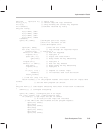
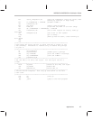
5 V
0.1 µF
(5)
3300 pF
OSC
IN
OSC
OUT
PLL
DAC
P
DAC
M
V
PP
V
DD
1N914
†
32 Ω
RESET
V
SS
5
5
1 µF
(20%)
1 kΩ
†
100 kΩ
5 V
1N914
Reset
Switch
To pin 2 of Scan Port Connector
†
To pin 1 of Scan Port Connector
†
(optional )
22 pF
22 pF
32 kHz
10 MΩ
10 MΩ
Minimum Circuit Configuration for the C614/P614 Using Crystal-Referenced Oscillator
MSP50C614/
MSP50P614
(optional )
(MSP50P614 only)