Architecture
A-3
MSP50C605 Preliminary Data
A.3.1 RAM
The MSP50C605 (like MSP50C614) has 640 17-bit words of internal data
memory (static RAM). This RAM occupies a space extending from 0 to 0x27F
in the address space.
A.3.2 ROM
The MSP50C605 contains 32K by 17-bit words of internal program ROM and
229,376 bytes by 8 bits (i.e., 1,835,008 bits) of slow data ROM. The program
ROM space is divided into three areas:
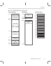
1) The initial 2K words of ROM (0x0000 – 0x07FF) is reserved for built in self-
test (BIST) that is provided by Texas Instruments during mass production.
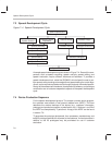
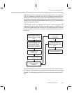
2) Customer can use the program ROM from address extending from
0x0800 to 0x7FFF. Restrictions on using certain program ROM location
is shown in Figure A–2.
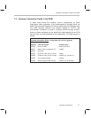
The Data ROM is a slower ROM dedicated only to hold data. Data ROM cannot
execute program instructions. The Data ROM locations start from 0x00000
and ends at 0x37FFF. The lower 16 bits of the address to be read is provided
into IO port DRA register (0x2C), the upper 2 bits goes into IO port DRP regis-
ter (0x08). After 1.5 instruction cycle delay, the 8 bit data appears at IO port
DRD (0x00). Discharging time is always 3 processor cycle and data is latched
to port DRD during this time. There is 3.5 page in MSP50C605; pages 0, 1, and
2 are full; page 3 is half. Using 1Kbps MELP algorithm, this ROM can provide
over 30 minutes of uninterrupted speech.
Port
Name
Description
IO
Address
Function
DRA Data ROM Address 0x2C write into this port to access 16 bit of
the data ROM address.
DRP Data ROM Page 0x08 write into this port to select ROM page
DRD
Data ROM Data 0x00 read this port to get data at specified
ROM page and address
A.3.3 I/O Pins
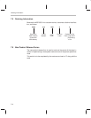
The MSP50C605 has 32 input/output pins. 24 of the pins are software confi-
gurable as either input or output (port C, D, and E). Eight of the pins are dedi-
cated as input pins with programmable pullout resistors (port F). These ports
are identical to the similar ports in MSP50C614, see Chapter 2 and Chapter 3
for details.


