Data Memory Address Unit
2-13
MSP50C614 Architecture
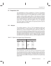
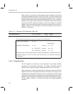
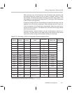
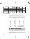
There are two-byte instructions, for example MOVB, which cause the proces-
sor to read or write data in a byte (8-bit) format. (The B appearing at the end
of MOVB designates it as an instruction, which uses byte-addressable argu-
ments.) The byte-addressable mode causes the hardware to read/write either
the upper or lower 8 bits of the 16-bit word based on the LSB of the address.
In this case, the address is a byte address, rather than a word address. Bits
0 through 7 within the word are used, so that a single byte is automatically right-
justified within the databus. Bits 8 through 15 may also be accessed as the up-
per byte at that same address.
A third data-addressing mode is the flag data mode, whereby, the instruction
operates on only the single flag bit (bit 16) at a given address. All flag mode
instructions execute in one instruction cycle. The flags can be referenced in
one of two addressing modes: 1) global address, whereby 64 global flags are
located at fixed locations in the first 64 RAM addresses, and 2) flag relative
address, whereby a reference is made relative to the current PAGE (R6). The
relative address supports 64 different flags whose PAGE-offset values are
stored in the PAGE register. The flag mode instructions cannot address
memory in the INDEX-relative modes. See Chapter 4,
Instructions
, for more
details.
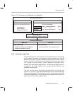
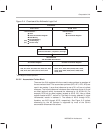
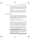
2.3.2 Data Memory Addressing Modes
The DMAU provides a powerful set of addressing modes to enhance the per-
formance and flexibility of the C614 core processor. The addressing modes for
RAM fall into three categories:
Direct addressing
Indirect addressing with post-modification
Relative addressing
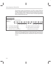
The relative addressing modes appear in three varieties:
Immediate Short, relative to the PAGE (R6) register.
The effective RAM address is: [*R6 + (a 7 bit direct offset)].
Relative to the INDEX (R5) register.
The effective RAM address is: [*R5 + (an indexed offset)].
Long Immediate, relative to the register base.
The effective RAM address is: [*R
x
+ (a 16 bit direct offset)].
Refer to Chapter 4,
Instructions
, for a full description of how these modes are
used in conjunction with various instructions.


