


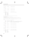


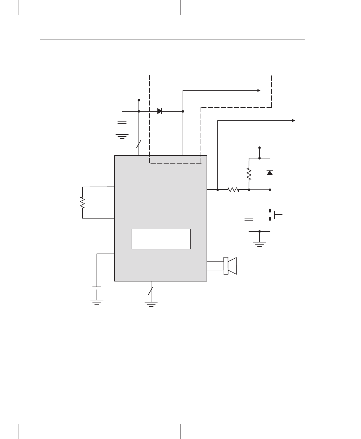
Application Circuits
6-2
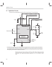
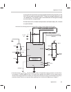
6.1 Application Circuits
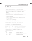
To pin 2 of Scan Port Connector
†
MSP50C614/
MSP50P614
To pin 1 of Scan Port Connector
†
(optional )
5 V
0.1 µF
(5)
R
REFERENCE
470 kΩ
(1%)
3300 pF
OSC
IN
OSC
OUT
PLL
DAC
P
DAC
M
V
PP
V
DD
1N914
†
32 Ω
RESET
V
SS
5
5
1 µF
20%
1 kΩ
†
100 kΩ
5 V
1N914
Reset
Switch
†
The diode across V
DD
and V
PP
may be omitted (shorted), if the application does not require use of the Scan Port Interface.
The same applies for the 1 kΩ resistor which appears at the RESET pin; the resistor may be shorted if not using the Scan
Port. However, the
footprint
for the resistor is
strongly
recommended for any C614 production board. Refer to the
Important
Note regarding Scan Port Bond Out
appearing in Chapter 7.
Minimum Circuit Configuration for the C614/P614 Using Resistor-Trimmed Oscillator
(optional )
(MSP50P614 only)
Note that there are 5 each of the pins V
DD
and V
SS
. Each of these should be
connected, with separate decoupling capacitors (0.1 µF) included for each
V
DD
.