C605 and C604 (Preliminary Information)
1-9
Introduction to the MSP50C614
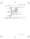
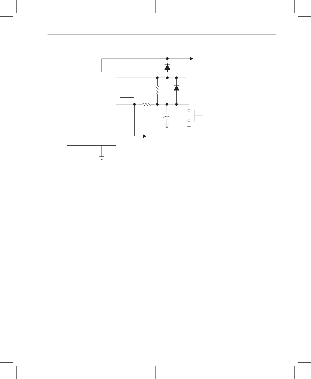
Figure 1–3. RESET Circuit
Reset
Switch
1 µF
(20%)
Inside the
MSP50P614
MSP50C614
V
DD
V
SS
100 kΩ
IN914
5 V
V
PP
To Pin 1 of Optional (Scanport)
Connector
RESET
1 kΩ
†
To Pin 2 of optional (scan port) connector
†
IN914
‡
(MSP50P614 only)
†
If it is necessary to use the software development tools to control the MSP50P614 in application board, the 1 kΩ resistor is need-
ed to allow the development tool to over drive the RESET circuit on the application board.
‡
This Diode can be omitted (shorted) if the application does not require use of the scanport interface. See Section 7.1.1 regarding
scan port bond out.


