I/O
3-3
Peripheral Functions
is 0x00 (all inputs). The state of the data registers after RESET low is unknown
(input state provided by external hardware).
The 8-bit width is the true size of the mapped location. This is independent of
the address spacing, which is greater than 8-bits. When writing to any of the
locations in the I/O address map, therefore, the bit-masking need only extend
across 8 bits. Within a 16-bit accumulator, the desired bits should be
right-justified. When reading from these locations to a 16-bit accumulator, the
IN instruction automatically clears the extra bits in excess of 8. The desired bits
in the result will be right-justified within the accumulator.
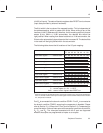
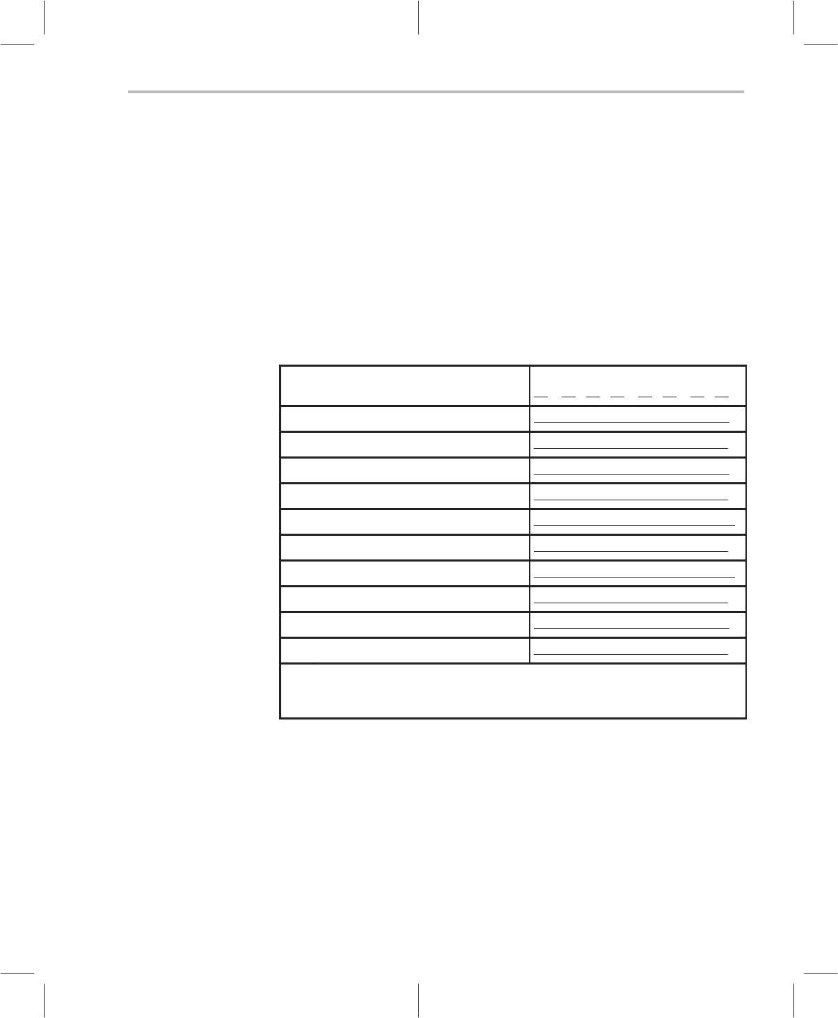
The following table shows the bit locations of the I/O port mapping:
(8-bit wide location)
07 06 05 04 03 02 01 00
A port data register address 0x00. . . . . A7 A6 A5 A4 A3 A2 A1 A0
A port control register address 0x04. . . C C C C C C C C
B port data register address 0x08. . . . . B7 B6 B5 B4 B3 B2 B1 B0
B port control register address 0x0C. . . C C C C C C C C
C port data register address 0x10. . . . . C7 C6 C5 C4 C3 C2 C1 C0
C port control register address 0x14. . . C C C C C C C C
D port data register address 0x18. . . . . D7 D6 D5 D4 D3 D2 D1 D0
D port control register
†
address 0x1C. . C C C C C C C C
E port data register address 0x20. . . . . E7 E6 E5 E4 E3 E2 E1 E0
E port control register address 0x24. . . C C C C C C C C
A7, B7, C7, D7, E7 : data register
C : control register (0 = IN, 1 = OUT)
0x00 : state of control register after RESET low
†
Ports D
4
and D
5
may be dedicated to the Comparator function, if the Comparator Enable bit is
set. If so, then bits 4 and 5 of the D port Control register
must
be CLEAR. Please refer to Section
3.3,
Comparator
, for details.
Port D
0
is connected to the branch condition COND1. Port D
1
is connected to
the branch condition COND2, assuming the comparator is disabled. Please
refer to Section 3.1.4,
Branch on D Port
, (and to Section 3.3,
Comparator
) for
more information. External interrupts can be caused by transitions on ports D
2
,
D
3
, D
4
, and D
5
. The interrupts associated with the D port are supported
whether those pins are programmed as inputs or as outputs.


