


TMS320F2809, TMS320F2808, TMS320F2806
TMS320F2802, TMS320F2801, TMS320C2802
TMS320C2801, TMS320F28016, TMS320F28015
SPRS230L–OCTOBER 2003–REVISED DECEMBER 2009
www.ti.com
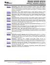
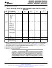
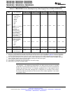
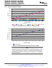
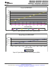
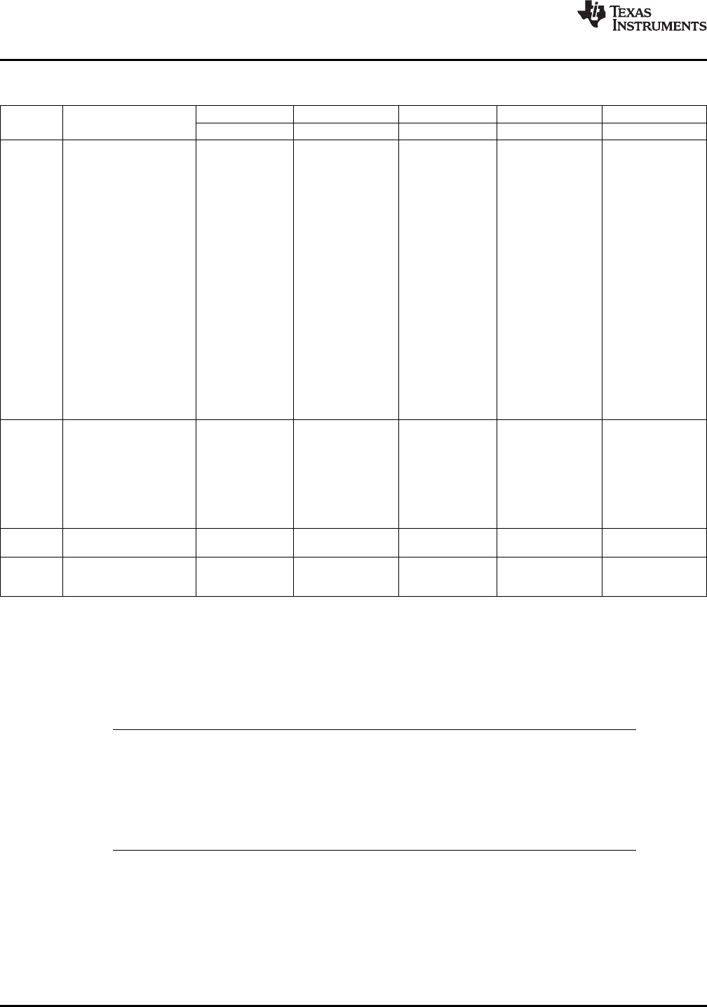
Table 6-2. TMS320F2806 Current Consumption by Power-Supply Pins at 100-MHz SYSCLKOUT
I
DD
I
DDIO
(1)
I
DD3VFL
(2)
I
DDA18
(3)
I
DDA33
(4)
MODE TEST CONDITIONS
TYP
(5)
MAX
(6)
TYP
(5)
MAX
(6)
TYP
(5)
MAX
(6)
TYP
(5)
MAX
(6)
TYP
(5)
MAX
(6)
The following peripheral
clocks are enabled:
• ePWM1/2/3/4/5/6
• eCAP1/2/3/4
• eQEP1/2
• eCAN-A
• SCI-A/B
• SPI-A
• ADC
Operational
• I2C
195 mA 230 mA 15 mA 27 mA 35 mA 40 mA 30 mA 38 mA 1.5 mA 2 mA
(Flash)
All PWM pins are toggled at
100 kHz.
All I/O pins are left
unconnected.
Data is continuously
transmitted out of the
SCI-A, SCI-B, and eCAN-A
ports. The hardware
multiplier is exercised.
Code is running out of flash
with 3 wait-states.
XCLKOUT is turned off
Flash is powered down.
XCLKOUT is turned off.
The following peripheral
clocks are enabled:
IDLE 75 mA 90 mA 500 μA 2 mA 2 μA 10 μA 5 μA 50 μA 15 μA 30 μA
• eCAN-A
• SCI-A
• SPI-A
• I2C
Flash is powered down.
STANDBY 6 mA 12 mA 100 μA 500 μA 2 μA 10 μA 5 μA 50 μA 15 μA 30 μA
Peripheral clocks are off.
Flash is powered down.
HALT Peripheral clocks are off. 70 μA 60 μA 120 μA 2 μA 10 μA 5 μA 50 μA 15 μA 30 μA
Input clock is disabled.
(1) I
DDIO
current is dependent on the electrical loading on the I/O pins.
(2) The I
DD3VFL
current indicated in this table is the flash read-current and does not include additional current for erase/write operations.
During flash programming, extra current is drawn from the V
DD
and V
DD3VFL
rails, as indicated in Table 6-45 . If the user application
involves on-board flash programming, this extra current must be taken into account while architecting the power-supply stage.
(3) I
DDA18
includes current into V
DD1A18
and V
DD2A18
pins. In order to realize the I
DDA18
currents shown for IDLE, STANDBY, and HALT,
clock to the ADC module must be turned off explicitly by writing to the PCLKCR0 register.
(4) I
DDA33
includes current into V
DDA2
and V
DDAIO
pins.
(5) TYP numbers are applicable over room temperature and nominal voltage.
(6) MAX numbers are at 125°C and MAX voltage.
NOTE
The peripheral - I/O multiplexing implemented in the 280x devices prevents all available
peripherals from being used at the same time. This is because more than one peripheral
function may share an I/O pin. It is, however, possible to turn on the clocks to all the
peripherals at the same time, although such a configuration is not useful. If this is done,
the current drawn by the device will be more than the numbers specified in the current
consumption tables.
96 Electrical Specifications Copyright © 2003–2009, Texas Instruments Incorporated
Submit Documentation Feedback
Product Folder Link(s): TMS320F2809 TMS320F2808 TMS320F2806 TMS320F2802 TMS320F2801 TMS320C2802
TMS320C2801 TMS320F28016 TMS320F28015