


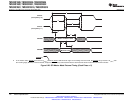
20
15
SPISIMO
SPISOMI
SPICLK
(clock polarity = 1)
SPICLK
(clock polarity = 0)
SPISIMO Data
Must Be Valid
SPISOMI Data Is Valid
19
16
14
13
12
SPISTE
(A)
TMS320F2809, TMS320F2808, TMS320F2806
TMS320F2802, TMS320F2801, TMS320C2802
TMS320C2801, TMS320F28016, TMS320F28015
www.ti.com
SPRS230L–OCTOBER 2003–REVISED DECEMBER 2009
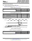
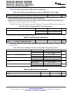
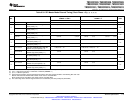
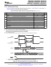
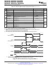
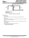
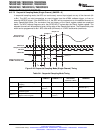
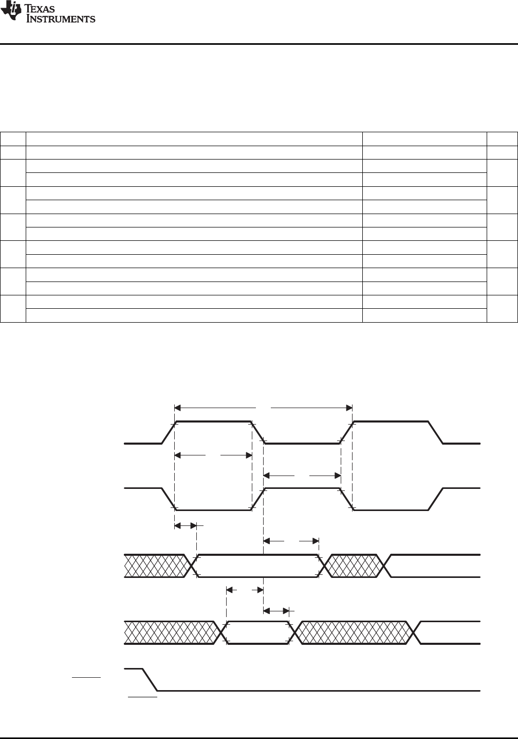
6.10.6 SPI Slave Mode Timing
Table 6-36 lists the slave mode external timing (clock phase = 0) and Table 6-37 (clock phase = 1).
Figure 6-22 and Figure 6-23 show the timing waveforms.
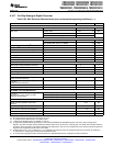
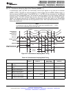
Table 6-36. SPI Slave Mode External Timing (Clock Phase = 0)
(1) (2) (3) (4) (5)
NO. MIN MAX UNIT
12 t
c(SPC)S
Cycle time, SPICLK 4t
c(LCO)
ns
t
w(SPCH)S
Pulse duration, SPICLK high (clock polarity = 0) 0.5t
c(SPC)S
– 10 0.5t
c(SPC)S
13 ns
t
w(SPCL)S
Pulse duration, SPICLK low (clock polarity = 1) 0.5t
c(SPC)S
– 10 0.5t
c(SPC)S
t
w(SPCL)S
Pulse duration, SPICLK low (clock polarity = 0) 0.5t
c(SPC)S
– 10 0.5t
c(SPC)S
14 ns
t
w(SPCH)S
Pulse duration, SPICLK high (clock polarity = 1) 0.5t
c(SPC)S
– 10 0.5t
c(SPC)S
t
d(SPCH-SOMI)S
Delay time, SPICLK high to SPISOMI valid (clock polarity = 0) 35
15 ns
t
d(SPCL-SOMI)S
Delay time, SPICLK low to SPISOMI valid (clock polarity = 1) 35
t
v(SPCL-SOMI)S
Valid time, SPISOMI data valid after SPICLK low (clock polarity = 0) 0.75t
c(SPC)S
16 ns
t
v(SPCH-SOMI)S
Valid time, SPISOMI data valid after SPICLK high (clock polarity = 1) 0.75t
c(SPC)S
t
su(SIMO-SPCL)S
Setup time, SPISIMO before SPICLK low (clock polarity = 0) 35
19 ns
t
su(SIMO-SPCH)S
Setup time, SPISIMO before SPICLK high (clock polarity = 1) 35
t
v(SPCL-SIMO)S
Valid time, SPISIMO data valid after SPICLK low (clock polarity = 0) 0.5t
c(SPC)S
– 10
20 ns
t
v(SPCH-SIMO)S
Valid time, SPISIMO data valid after SPICLK high (clock polarity = 1) 0.5t
c(SPC)S
– 10
(1) The MASTER / SLAVE bit (SPICTL.2) is cleared and the CLOCK PHASE bit (SPICTL.3) is cleared.
(2) t
c(SPC)
= SPI clock cycle time = LSPCLK/4 or LSPCLK/(SPIBRR + 1)
(3) Internal clock prescalers must be adjusted such that the SPI clock speed is limited to the following SPI clock rate:
Master mode transmit 25-MHz MAX, master mode receive 12.5-MHz MAX
Slave mode transmit 12.5-MHz MAX, slave mode receive 12.5-MHz MAX.
(4) t
c(LCO)
= LSPCLK cycle time
(5) The active edge of the SPICLK signal referenced is controlled by the CLOCK POLARITY bit (SPICCR.6).
A. In the slave mode, the SPISTE signal should be asserted low at least 0.5t
c(SPC)
(minimum) before the valid SPI clock
edge and remain low for at least 0.5t
c(SPC)
after the receiving edge (SPICLK) of the last data bit.
Figure 6-22. SPI Slave Mode External Timing (Clock Phase = 0)
Copyright © 2003–2009, Texas Instruments Incorporated Electrical Specifications 123
Submit Documentation Feedback
Product Folder Link(s): TMS320F2809 TMS320F2808 TMS320F2806 TMS320F2802 TMS320F2801 TMS320C2802
TMS320C2801 TMS320F28016 TMS320F28015