


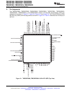
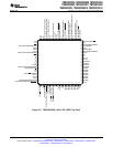
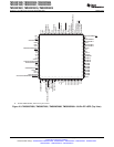
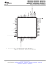

TMS320F2809, TMS320F2808, TMS320F2806
TMS320F2802, TMS320F2801, TMS320C2802
TMS320C2801, TMS320F28016, TMS320F28015
SPRS230L–OCTOBER 2003–REVISED DECEMBER 2009
www.ti.com
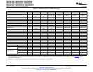
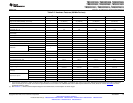
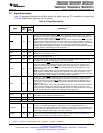
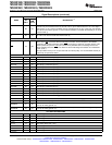
Signal Descriptions (continued)
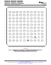
PIN NO.
GGM/
NAME DESCRIPTION
(1)
PZ
ZGM
PIN #
BALL #
Internal/External Oscillator Input. To use the internal oscillator, a quartz crystal or a ceramic
resonator may be connected across X1 and X2. The X1 pin is referenced to the 1.8-V core digital
X1 88 E6 power supply. A 1.8-V external oscillator may be connected to the X1 pin. In this case, the XCLKIN
pin must be connected to ground. If a 3.3-V external oscillator is used with the XCLKIN pin, X1 must
be tied to GND. (I)
Internal Oscillator Output. A quartz crystal or a ceramic resonator may be connected across X1 and
X2 86 C6
X2. If X2 is not used it must be left unconnected. (O)
RESET
Device Reset (in) and Watchdog Reset (out).
Device reset. XRS causes the device to terminate execution. The PC will point to the address
contained at the location 0x3FFFC0. When XRS is brought to a high level, execution begins at the
location pointed to by the PC. This pin is driven low by the DSP when a watchdog reset occurs.
XRS 78 B8
During watchdog reset, the XRS pin is driven low for the watchdog reset duration of 512 OSCCLK
cycles. (I/OD, ↑)
The output buffer of this pin is an open-drain with an internal pullup. It is recommended that this pin
be driven by an open-drain device.
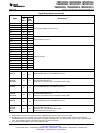
ADC SIGNALS
ADCINA7 16 F3 ADC Group A, Channel 7 input (I)
ADCINA6 17 F4 ADC Group A, Channel 6 input (I)
ADCINA5 18 G4 ADC Group A, Channel 5 input (I)
ADCINA4 19 G1 ADC Group A, Channel 4 input (I)
ADCINA3 20 G2 ADC Group A, Channel 3 input (I)
ADCINA2 21 G3 ADC Group A, Channel 2 input (I)
ADCINA1 22 H1 ADC Group A, Channel 1 input (I)
ADCINA0 23 H2 ADC Group A, Channel 0 input (I)
ADCINB7 34 K5 ADC Group B, Channel 7 input (I)
ADCINB6 33 H4 ADC Group B, Channel 6 input (I)
ADCINB5 32 K4 ADC Group B, Channel 5 input (I)
ADCINB4 31 J4 ADC Group B, Channel 4 input (I)
ADCINB3 30 K3 ADC Group B, Channel 3 input (I)
ADCINB2 29 H3 ADC Group B, Channel 2 input (I)
ADCINB1 28 J3 ADC Group B, Channel 1 input (I)
ADCINB0 27 K2 ADC Group B, Channel 0 input (I)
ADCLO 24 J1 Low Reference (connect to analog ground) (I)
ADCRESEXT 38 F5 ADC External Current Bias Resistor. Connect a 22-kΩ resistor to analog ground.
ADCREFIN 35 J5 External reference input (I)
Internal Reference Positive Output. Requires a low ESR (50 mΩ - 1.5 Ω) ceramic bypass capacitor
ADCREFP 37 G5
of 2.2 μF to analog ground. (O)
Internal Reference Medium Output. Requires a low ESR (50 mΩ - 1.5 Ω) ceramic bypass capacitor
ADCREFM 36 H5
of 2.2 μF to analog ground. (O)
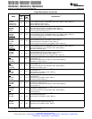
CPU AND I/O POWER PINS
V
DDA2
15 F2 ADC Analog Power Pin (3.3 V)
V
SSA2
14 F1 ADC Analog Ground Pin
V
DDAIO
26 J2 ADC Analog I/O Power Pin (3.3 V)
V
SSAIO
25 K1 ADC Analog I/O Ground Pin
V
DD1A18
12 E4 ADC Analog Power Pin (1.8 V)
V
SS1AGND
13 E5 ADC Analog Ground Pin
V
DD2A18
40 J6 ADC Analog Power Pin (1.8 V)
V
SS2AGND
39 K6 ADC Analog Ground Pin
20 Introduction Copyright © 2003–2009, Texas Instruments Incorporated
Submit Documentation Feedback
Product Folder Link(s): TMS320F2809 TMS320F2808 TMS320F2806 TMS320F2802 TMS320F2801 TMS320C2802
TMS320C2801 TMS320F28016 TMS320F28015