


TMS320F2809, TMS320F2808, TMS320F2806
TMS320F2802, TMS320F2801, TMS320C2802
TMS320C2801, TMS320F28016, TMS320F28015
SPRS230L–OCTOBER 2003–REVISED DECEMBER 2009
www.ti.com
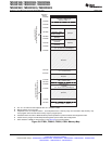
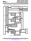
3.2.11 Peripheral Interrupt Expansion (PIE) Block
The PIE block serves to multiplex numerous interrupt sources into a smaller set of interrupt inputs. The
PIE block can support up to 96 peripheral interrupts. On the 280x, 43 of the possible 96 interrupts are
used by peripherals. The 96 interrupts are grouped into blocks of 8 and each group is fed into 1 of
12 CPU interrupt lines (INT1 to INT12). Each of the 96 interrupts is supported by its own vector stored in a
dedicated RAM block that can be overwritten by the user. The vector is automatically fetched by the CPU
on servicing the interrupt. It takes 8 CPU clock cycles to fetch the vector and save critical CPU registers.
Hence the CPU can quickly respond to interrupt events. Prioritization of interrupts is controlled in
hardware and software. Each individual interrupt can be enabled/disabled within the PIE block.
3.2.12 External Interrupts (XINT1, XINT2, XNMI)
The 280x supports three masked external interrupts (XINT1, XINT2, XNMI). XNMI can be connected to
the INT13 or NMI interrupt of the CPU. Each of the interrupts can be selected for negative, positive, or
both negative and positive edge triggering and can also be enabled/disabled (including the XNMI). The
masked interrupts also contain a 16-bit free running up counter, which is reset to zero when a valid
interrupt edge is detected. This counter can be used to accurately time stamp the interrupt. Unlike the
281x devices, there are no dedicated pins for the external interrupts. Rather, any Port A GPIO pin can be
configured to trigger any external interrupt.
3.2.13 Oscillator and PLL
The 280x can be clocked by an external oscillator or by a crystal attached to the on-chip oscillator circuit.
A PLL is provided supporting up to 10 input-clock-scaling ratios. The PLL ratios can be changed on-the-fly
in software, enabling the user to scale back on operating frequency if lower power operation is desired.
Refer to the Electrical Specification section for timing details. The PLL block can be set in bypass mode.
3.2.14 Watchdog
The 280x devices contain a watchdog timer. The user software must regularly reset the watchdog counter
within a certain time frame; otherwise, the watchdog will generate a reset to the processor. The watchdog
can be disabled if necessary.
3.2.15 Peripheral Clocking
The clocks to each individual peripheral can be enabled/disabled so as to reduce power consumption
when a peripheral is not in use. Additionally, the system clock to the serial ports (except I2C and eCAN)
and the ADC blocks can be scaled relative to the CPU clock. This enables the timing of peripherals to be
decoupled from increasing CPU clock speeds.
3.2.16 Low-Power Modes
The 280x devices are full static CMOS devices. Three low-power modes are provided:
IDLE: Place CPU into low-power mode. Peripheral clocks may be turned off selectively and
only those peripherals that need to function during IDLE are left operating. An
enabled interrupt from an active peripheral or the watchdog timer will wake the
processor from IDLE mode.
STANDBY: Turns off clock to CPU and peripherals. This mode leaves the oscillator and PLL
functional. An external interrupt event will wake the processor and the peripherals.
Execution begins on the next valid cycle after detection of the interrupt event
HALT: Turns off the internal oscillator. This mode basically shuts down the device and
places it in the lowest possible power consumption mode. A reset or external signal
can wake the device from this mode.
38 Functional Overview Copyright © 2003–2009, Texas Instruments Incorporated
Submit Documentation Feedback
Product Folder Link(s): TMS320F2809 TMS320F2808 TMS320F2806 TMS320F2802 TMS320F2801 TMS320C2802
TMS320C2801 TMS320F28016 TMS320F28015