


TMS320F2809, TMS320F2808, TMS320F2806
TMS320F2802, TMS320F2801, TMS320C2802
TMS320C2801, TMS320F28016, TMS320F28015
SPRS230L–OCTOBER 2003–REVISED DECEMBER 2009
www.ti.com
3.2 Brief Descriptions
3.2.1 C28x CPU
The C28x™ DSP generation is the newest member of the TMS320C2000™ DSP platform. The C28x is a
very efficient C/C++ engine, enabling users to develop not only their system control software in a
high-level language, but also enables math algorithms to be developed using C/C++. The C28x is as
efficient in DSP math tasks as it is in system control tasks that typically are handled by microcontroller
devices. This efficiency removes the need for a second processor in many systems. The 32 x 32-bit MAC
capabilities of the C28x and its 64-bit processing capabilities, enable the C28x to efficiently handle higher
numerical resolution problems that would otherwise demand a more expensive floating-point processor
solution. Add to this the fast interrupt response with automatic context save of critical registers, resulting in
a device that is capable of servicing many asynchronous events with minimal latency. The C28x has an
8-level-deep protected pipeline with pipelined memory accesses. This pipelining enables the C28x to
execute at high speeds without resorting to expensive high-speed memories. Special branch-look-ahead
hardware minimizes the latency for conditional discontinuities. Special store conditional operations further
improve performance.
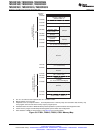
3.2.2 Memory Bus (Harvard Bus Architecture)
As with many DSP type devices, multiple busses are used to move data between the memories and
peripherals and the CPU. The C28x memory bus architecture contains a program read bus, data read bus
and data write bus. The program read bus consists of 22 address lines and 32 data lines. The data read
and write busses consist of 32 address lines and 32 data lines each. The 32-bit-wide data busses enable
single cycle 32-bit operations. The multiple bus architecture, commonly termed Harvard Bus, enables the
C28x to fetch an instruction, read a data value and write a data value in a single cycle. All peripherals and
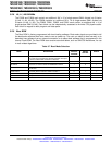
memories attached to the memory bus will prioritize memory accesses. Generally, the priority of memory
bus accesses can be summarized as follows:
Highest: Data Writes (Simultaneous data and program writes cannot occur on the
memory bus.)
Program Writes (Simultaneous data and program writes cannot occur on the
memory bus.)
Data Reads
Program (Simultaneous program reads and fetches cannot occur on the
Reads memory bus.)
Lowest: Fetches (Simultaneous program reads and fetches cannot occur on the
memory bus.)
3.2.3 Peripheral Bus
To enable migration of peripherals between various Texas Instruments (TI) DSP family of devices, the
280x devices adopt a peripheral bus standard for peripheral interconnect. The peripheral bus bridge
multiplexes the various busses that make up the processor Memory Bus into a single bus consisting of
16 address lines and 16 or 32 data lines and associated control signals. Two versions of the peripheral
bus are supported on the 280x. One version only supports 16-bit accesses (called peripheral frame 2).
The other version supports both 16- and 32-bit accesses (called peripheral frame 1).
34 Functional Overview Copyright © 2003–2009, Texas Instruments Incorporated
Submit Documentation Feedback
Product Folder Link(s): TMS320F2809 TMS320F2808 TMS320F2806 TMS320F2802 TMS320F2801 TMS320C2802
TMS320C2801 TMS320F28016 TMS320F28015