


TMS320F2809, TMS320F2808, TMS320F2806
TMS320F2802, TMS320F2801, TMS320C2802
TMS320C2801, TMS320F28016, TMS320F28015
SPRS230L–OCTOBER 2003–REVISED DECEMBER 2009
www.ti.com
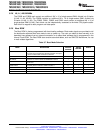
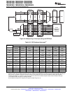
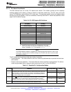
Table 3-10. Peripheral Frame 2 Registers
(1) (2)
NAME ADDRESS RANGE SIZE (x16) ACCESS TYPE
System Control Registers 0x7010 – 0x702F 32 EALLOW Protected
SPI-A Registers 0x7040 – 0x704F 16
SCI-A Registers 0x7050 – 0x705F 16
External Interrupt Registers 0x7070 – 0x707F 16
ADC Registers 0x7100 – 0x711F 32
SPI-B Registers 0x7740 – 0x774F 16 Not EALLOW Protected
SCI-B Registers 0x7750 – 0x775F 16
SPI-C Registers 0x7760 – 0x776F 16
SPI-D Registers 0x7780 – 0x778F 16
I2C Registers 0x7900 – 0x792F 48
(1) Peripheral Frame 2 only allows 16-bit accesses. All 32-bit accesses are ignored (invalid data may be returned or written).
(2) Missing segments of memory space are reserved and should not be used in applications.
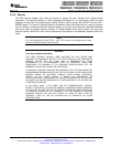
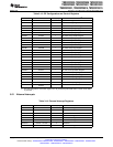
3.4 Device Emulation Registers
These registers are used to control the protection mode of the C28x CPU and to monitor some critical
device signals. The registers are defined in Table 3-11.
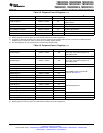
Table 3-11. Device Emulation Registers
ADDRESS
NAME SIZE (x16) DESCRIPTION
RANGE
0x0880
DEVICECNF 2 Device Configuration Register
0x0881
PARTID 0x0882 1 Part ID Register 0x002C
(1)
- F2801
0x0024 – F2802
0x0034 – F2806
0x003C – F2808
0x00FE – F2809
0x0014 – F28016
0x001C – F28015
0xFF2C – C2801
0xFF24 – C2802
REVID 0x0883 1 Revision ID Register 0x0000 – Silicon Rev. 0 – TMX
0x0001 – Silicon Rev. A – TMX
0x0002 – Silicon Rev. B – TMS
0x0003 – Silicon Rev. C – TMS
Revision ID Register 0x0000 – Silicon rev. 0 – TMS (F2809 only)
PROTSTART 0x0884 1 Block Protection Start Address Register
PROTRANGE 0x0885 1 Block Protection Range Address Register
(1) The first byte (00) denotes flash devices. FF denotes ROM devices. Other values are reserved for future devices.
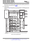
3.5 Interrupts
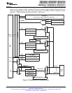
Figure 3-7 shows how the various interrupt sources are multiplexed within the 280x devices.
Eight PIE block interrupts are grouped into one CPU interrupt. In total, 12 CPU interrupt groups, with
8 interrupts per group equals 96 possible interrupts. On the 280x, 43 of these are used by peripherals as
shown in Table 3-12.
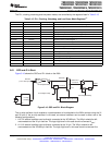
The TRAP #VectorNumber instruction transfers program control to the interrupt service routine
corresponding to the vector specified. TRAP #0 attempts to transfer program control to the address
pointed to by the reset vector. The PIE vector table does not, however, include a reset vector. Therefore,
TRAP #0 should not be used when the PIE is enabled. Doing so will result in undefined behavior.
42 Functional Overview Copyright © 2003–2009, Texas Instruments Incorporated
Submit Documentation Feedback
Product Folder Link(s): TMS320F2809 TMS320F2808 TMS320F2806 TMS320F2802 TMS320F2801 TMS320C2802
TMS320C2801 TMS320F28016 TMS320F28015