


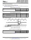
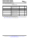
t
d(IDLE−XCOL)
X1/X2
or XCLKIN
XCLKOUT
HALT HALT
Wake-up Latency
Flushing Pipeline
t
d(WAKE−HALT)
(A)
(B)
(C)
(D)
Device
Status
(E)
(G)
(F)
PLL Lock-up Time
Normal
Execution
t
w(WAKE-GPIO)
t
p
GPIOn
Oscillator Start-up Time
TMS320F2809, TMS320F2808, TMS320F2806
TMS320F2802, TMS320F2801, TMS320C2802
TMS320C2801, TMS320F28016, TMS320F28015
SPRS230L–OCTOBER 2003–REVISED DECEMBER 2009
www.ti.com
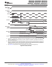
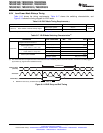
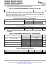
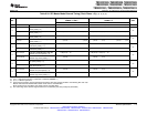
Table 6-20. HALT Mode Timing Requirements
MIN NOM MAX UNIT
t
w(WAKE-GPIO)
Pulse duration, GPIO wake-up signal t
oscst
+ 2t
c(OSCCLK)
(1)
cycles
t
w(WAKE-XRS)
Pulse duration, XRS wakeup signal t
oscst
+ 8t
c(OSCCLK)
cycles
(1) See Table 6-13 for an explanation of t
oscst
.
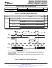
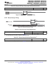
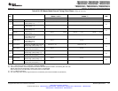
Table 6-21. HALT Mode Switching Characteristics
PARAMETER MIN TYP MAX UNIT
t
d(IDLE-XCOL)
Delay time, IDLE instruction executed to XCLKOUT low 32t
c(SCO)
45t
c(SCO)
cycles
t
p
PLL lock-up time 131072t
c(OSCCLK)
cycles
Delay time, PLL lock to program execution resume
1125t
c(SCO)
cycles
• Wake up from flash
t
d(WAKE-HALT)
– Flash module in sleep state
35t
c(SCO)
cycles
• Wake up from SARAM
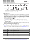
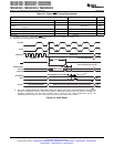
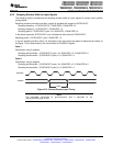
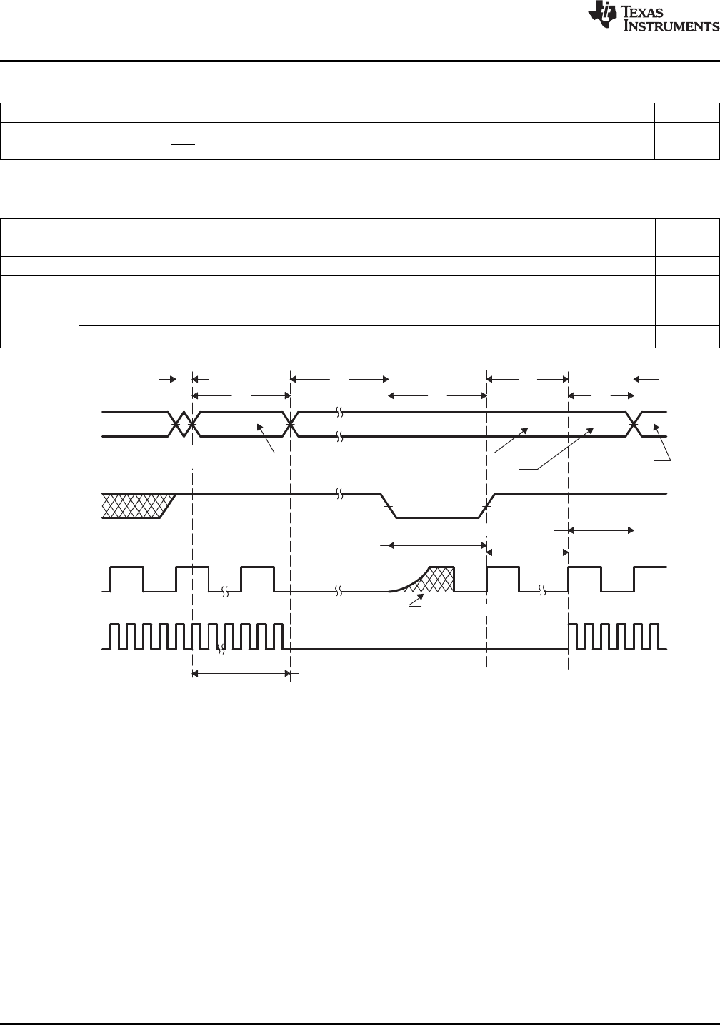
A. IDLE instruction is executed to put the device into HALT mode.
B. The PLL block responds to the HALT signal. SYSCLKOUT is held for approximately 32 cycles (if CLKINDIV = 0) or
64 cycles (if CLKINDIV = 1) before the oscillator is turned off and the CLKIN to the core is stopped. This delay
enables the CPU pipe and any other pending operations to flush properly.
C. Clocks to the peripherals are turned off and the PLL is shut down. If a quartz crystal or ceramic resonator is used as
the clock source, the internal oscillator is shut down as well. The device is now in HALT mode and consumes
absolute minimum power.
D. When the GPIOn pin (used to bring the device out of HALT) is driven low, the oscillator is turned on and the oscillator
wake-up sequence is initiated. The GPIO pin should be driven high only after the oscillator has stabilized. This
enables the provision of a clean clock signal during the PLL lock sequence. Since the falling edge of the GPIO pin
asynchronously begins the wakeup process, care should be taken to maintain a low noise environment prior to
entering and during HALT mode.
E. Once the oscillator has stabilized, the PLL lock sequence is initiated, which takes 131,072 OSCCLK (X1/X2 or X1 or
XCLKIN) cycles. Note that these 131,072 clock cycles are applicable even when the PLL is disabled (i.e., code
execution will be delayed by this duration even when the PLL is disabled).
F. Clocks to the core and peripherals are enabled. The HALT mode is now exited. The device will respond to the
interrupt (if enabled), after a latency.
G. Normal operation resumes.
Figure 6-16. HALT Wake-Up Using GPIOn
114 Electrical Specifications Copyright © 2003–2009, Texas Instruments Incorporated
Submit Documentation Feedback
Product Folder Link(s): TMS320F2809 TMS320F2808 TMS320F2806 TMS320F2802 TMS320F2801 TMS320C2802
TMS320C2801 TMS320F28016 TMS320F28015