


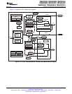
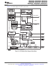
GPxDAT (read)
Input
Qualification
GPxMUX1/2
High Impedance
Output Control
GPIOx pin
XRS
0 = Input, 1 = Output
Low Power
Modes Block
GPxDIR (latch)
Peripheral 2 Input
Peripheral 3 Input
Peripheral 1 Output
Peripheral 2 Output
Peripheral 3 Output
Peripheral 1 Output Enable
Peripheral 2 Output Enable
Peripheral 3 Output Enable
00
01
10
11
00
01
10
11
00
01
10
11
GPxCTRL
Peripheral 1 Input
N/C
GPxPUD
LPMCR0
Internal
Pullup
GPIOLMPSEL
GPxQSEL1/2
GPxSET
GPxDAT (latch)
GPxCLEAR
GPxTOGGLE
GPIOXINT1SEL
GPIOXINT2SEL
GPIOXNMISEL
= Default at Reset
PIE
External Interrupt
MUX
Asynchronous
path
Asynchronous path
TMS320F2809, TMS320F2808, TMS320F2806
TMS320F2802, TMS320F2801, TMS320C2802
TMS320C2801, TMS320F28016, TMS320F28015
SPRS230L–OCTOBER 2003–REVISED DECEMBER 2009
www.ti.com
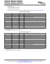
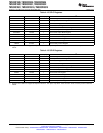
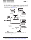
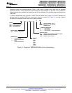
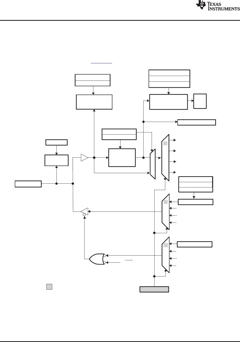
4.11 GPIO MUX
On the 280x, the GPIO MUX can multiplex up to three independent peripheral signals on a single GPIO
pin in addition to providing individual pin bit-banging IO capability. The GPIO MUX block diagram per pin
is shown in Figure 4-16. Because of the open drain capabilities of the I2C pins, the GPIO MUX block
diagram for these pins differ. See the TMS320x280x, 2801x, 2804x DSP System Control and Interrupts
Reference Guide (literature number SPRU712) for details.
A. x stands for the port, either A or B. For example, GPxDIR refers to either the GPADIR and GPBDIR register
depending on the particular GPIO pin selected.
B. GPxDAT latch/read are accessed at the same memory location.
Figure 4-16. GPIO MUX Block Diagram
82 Peripherals Copyright © 2003–2009, Texas Instruments Incorporated
Submit Documentation Feedback
Product Folder Link(s): TMS320F2809 TMS320F2808 TMS320F2806 TMS320F2802 TMS320F2801 TMS320C2802
TMS320C2801 TMS320F28016 TMS320F28015