


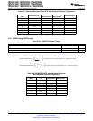
Analog Input on
Channel Ax or Bx
ADC Clock
Sample and Hold
SH Pulse
SMODE Bit
t
dschx_n
t
dschx_n+1
Sample n
Sample n+1
Sample n+2
t
SH
ADC Event Trigger from
ePWM or Other Sources
t
d(SH)
TMS320F2809, TMS320F2808, TMS320F2806
TMS320F2802, TMS320F2801, TMS320C2802
TMS320C2801, TMS320F28016, TMS320F28015
SPRS230L–OCTOBER 2003–REVISED DECEMBER 2009
www.ti.com
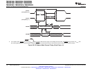
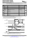
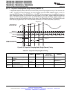
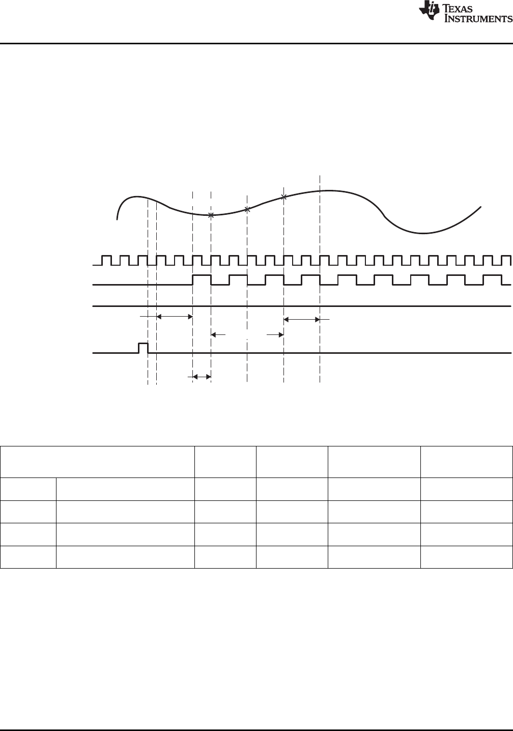
6.10.7.3 Sequential Sampling Mode (Single-Channel) (SMODE = 0)
In sequential sampling mode, the ADC can continuously convert input signals on any of the channels (Ax
to Bx). The ADC can start conversions on event triggers from the ePWM, software trigger, or from an
external ADCSOC signal. If the SMODE bit is 0, the ADC will do conversions on the selected channel on
every Sample/Hold pulse. The conversion time and latency of the Result register update are explained
below. The ADC interrupt flags are set a few SYSCLKOUT cycles after the Result register update. The
selected channels will be sampled at every falling edge of the Sample/Hold pulse. The Sample/Hold pulse
width can be programmed to be 1 ADC clock wide (minimum) or 16 ADC clocks wide (maximum).
Figure 6-26. Sequential Sampling Mode (Single-Channel) Timing
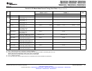
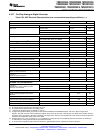
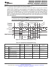
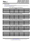
Table 6-41. Sequential Sampling Mode Timing
AT 12.5 MHz
SAMPLE n SAMPLE n + 1 ADC CLOCK, REMARKS
t
c(ADCCLK)
= 80 ns
t
d(SH)
Delay time from event trigger to 2.5t
c(ADCCLK)
sampling
t
SH
Sample/Hold width/Acquisition (1 + Acqps) * 80 ns with Acqps = 0 Acqps value = 0–15
Width t
c(ADCCLK)
ADCTRL1[8:11]
t
d(schx_n)
Delay time for first result to appear 4t
c(ADCCLK)
320 ns
in Result register
t
d(schx_n+1)
Delay time for successive results to (2 + Acqps) * 160 ns
appear in Result register t
c(ADCCLK)
128 Electrical Specifications Copyright © 2003–2009, Texas Instruments Incorporated
Submit Documentation Feedback
Product Folder Link(s): TMS320F2809 TMS320F2808 TMS320F2806 TMS320F2802 TMS320F2801 TMS320C2802
TMS320C2801 TMS320F28016 TMS320F28015