


TMS320F2809, TMS320F2808, TMS320F2806
TMS320F2802, TMS320F2801, TMS320C2802
TMS320C2801, TMS320F28016, TMS320F28015
SPRS230L–OCTOBER 2003–REVISED DECEMBER 2009
www.ti.com
Contents
1 F280x, F2801x, C280x DSPs .................................................................................................. 9
1.1 Features ...................................................................................................................... 9
1.2 Getting Started ............................................................................................................. 10
2 Introduction ...................................................................................................................... 11
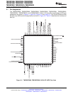
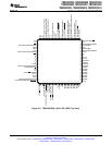
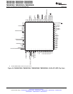
2.1 Pin Assignments ........................................................................................................... 14
2.2 Signal Descriptions ........................................................................................................ 19
3 Functional Overview .......................................................................................................... 25
3.1 Memory Maps .............................................................................................................. 26
3.2 Brief Descriptions .......................................................................................................... 34
3.2.1 C28x CPU ....................................................................................................... 34
3.2.2 Memory Bus (Harvard Bus Architecture) .................................................................... 34
3.2.3 Peripheral Bus .................................................................................................. 34
3.2.4 Real-Time JTAG and Analysis ................................................................................ 35
3.2.5 Flash ............................................................................................................. 35
3.2.6 ROM .............................................................................................................. 35
3.2.7 M0, M1 SARAMs ............................................................................................... 35
3.2.8 L0, L1, H0 SARAMs ............................................................................................ 36
3.2.9 Boot ROM ....................................................................................................... 36
3.2.10 Security .......................................................................................................... 37
3.2.11 Peripheral Interrupt Expansion (PIE) Block ................................................................. 38
3.2.12 External Interrupts (XINT1, XINT2, XNMI) .................................................................. 38
3.2.13 Oscillator and PLL .............................................................................................. 38
3.2.14 Watchdog ........................................................................................................ 38
3.2.15 Peripheral Clocking ............................................................................................. 38
3.2.16 Low-Power Modes .............................................................................................. 38
3.2.17 Peripheral Frames 0, 1, 2 (PFn) .............................................................................. 39
3.2.18 General-Purpose Input/Output (GPIO) Multiplexer ......................................................... 39
3.2.19 32-Bit CPU-Timers (0, 1, 2) ................................................................................... 39
3.2.20 Control Peripherals ............................................................................................. 39
3.2.21 Serial Port Peripherals ......................................................................................... 40
3.3 Register Map ............................................................................................................... 40
3.4 Device Emulation Registers .............................................................................................. 42
3.5 Interrupts .................................................................................................................... 42
3.5.1 External Interrupts .............................................................................................. 45
3.6 System Control ............................................................................................................ 46
3.6.1 OSC and PLL Block ............................................................................................ 47
3.6.1.1 External Reference Oscillator Clock Option .................................................... 48
3.6.1.2 PLL-Based Clock Module ......................................................................... 49
3.6.1.3 Loss of Input Clock ................................................................................ 50
3.6.2 Watchdog Block ................................................................................................. 51
3.7 Low-Power Modes Block ................................................................................................. 52
4 Peripherals ....................................................................................................................... 53
4.1 32-Bit CPU-Timers 0/1/2 ................................................................................................. 53
4.2 Enhanced PWM Modules (ePWM1/2/3/4/5/6) ......................................................................... 55
4.3 Hi-Resolution PWM (HRPWM) .......................................................................................... 58
2 Contents Copyright © 2003–2009, Texas Instruments Incorporated