


TMS320F2809, TMS320F2808, TMS320F2806
TMS320F2802, TMS320F2801, TMS320C2802
TMS320C2801, TMS320F28016, TMS320F28015
www.ti.com
SPRS230L–OCTOBER 2003–REVISED DECEMBER 2009
6.4 Current Consumption
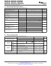
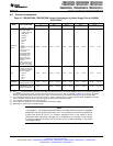
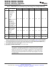
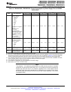
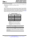
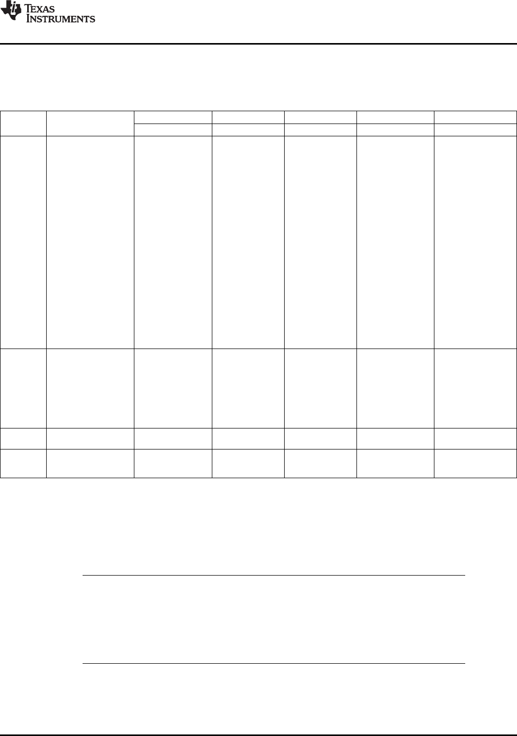
Table 6-1. TMS320F2809, TMS320F2808 Current Consumption by Power-Supply Pins at 100-MHz
SYSCLKOUT
I
DD
I
DDIO
(1)
I
DD3VFL
(2)
I
DDA18
(3)
I
DDA33
(4)
MODE TEST CONDITIONS
TYP
(5)
MAX
(6)
TYP
(5)
MAX
(6)
TYP MAX
(6)
TYP
(5)
MAX
(6)
TYP
(5)
MAX
(6)
The following peripheral
clocks are enabled:
• ePWM1/2/3/4/5/6
• eCAP1/2/3/4
• eQEP1/2
• eCAN-A
• SCI-A/B
• SPI-A
• ADC
• I2C
Operational
195 mA 230 mA 15 mA 27 mA 35 mA 40 mA 30 mA 38 mA 1.5 mA 2 mA
All PWM pins are toggled
(Flash)
at 100 kHz.
All I/O pins are left
unconnected.
Data is continuously
transmitted out of the
SCI-A, SCI-B, and
eCAN-A ports. The
hardware multiplier is
exercised.
Code is running out of
flash with 3 wait-states.
XCLKOUT is turned off.
Flash is powered down.
XCLKOUT is turned off.
The following peripheral
clocks are enabled:
IDLE 75 mA 90 mA 500 μA 2 mA 2 μA 10 μA 5 μA 50 μA 15μA 30 μA
• eCAN-A
• SCI-A
• SPI-A
• I2C
Flash is powered down.
STANDBY 6 mA 12 mA 100 μA 500 μA 2 μA 10 μA 5 μA 50 μA 15 μA 30 μA
Peripheral clocks are off.
Flash is powered down.
HALT Peripheral clocks are off. 70 μA 60 μA 120 μA 2 μA 10 μA 5 μA 50 μA 15 μA 30 μA
Input clock is disabled.
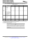
(1) I
DDIO
current is dependent on the electrical loading on the I/O pins.
(2) The I
DD3VFL
current indicated in this table is the flash read-current and does not include additional current for erase/write operations.
During flash programming, extra current is drawn from the V
DD
and V
DD3VFL
rails, as indicated in Table 6-45 . If the user application
involves on-board flash programming, this extra current must be taken into account while architecting the power-supply stage.
(3) I
DDA18
includes current into V
DD1A18
and V
DD2A18
pins. In order to realize the I
DDA18
currents shown for IDLE, STANDBY, and HALT,
clock to the ADC module must be turned off explicitly by writing to the PCLKCR0 register.
(4) I
DDA33
includes current into V
DDA2
and V
DDAIO
pins.
(5) TYP numbers are applicable over room temperature and nominal voltage.
(6) MAX numbers are at 125°C and MAX voltage.
NOTE
The peripheral - I/O multiplexing implemented in the 280x devices prevents all available
peripherals from being used at the same time. This is because more than one peripheral
function may share an I/O pin. It is, however, possible to turn on the clocks to all the
peripherals at the same time, although such a configuration is not useful. If this is done,
the current drawn by the device will be more than the numbers specified in the current
consumption tables.
Copyright © 2003–2009, Texas Instruments Incorporated Electrical Specifications 95
Submit Documentation Feedback
Product Folder Link(s): TMS320F2809 TMS320F2808 TMS320F2806 TMS320F2802 TMS320F2801 TMS320C2802
TMS320C2801 TMS320F28016 TMS320F28015