


TMS320F2809, TMS320F2808, TMS320F2806
TMS320F2802, TMS320F2801, TMS320C2802
TMS320C2801, TMS320F28016, TMS320F28015
SPRS230L–OCTOBER 2003–REVISED DECEMBER 2009
www.ti.com
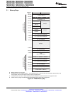
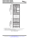
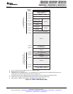
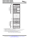
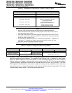
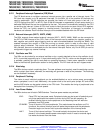
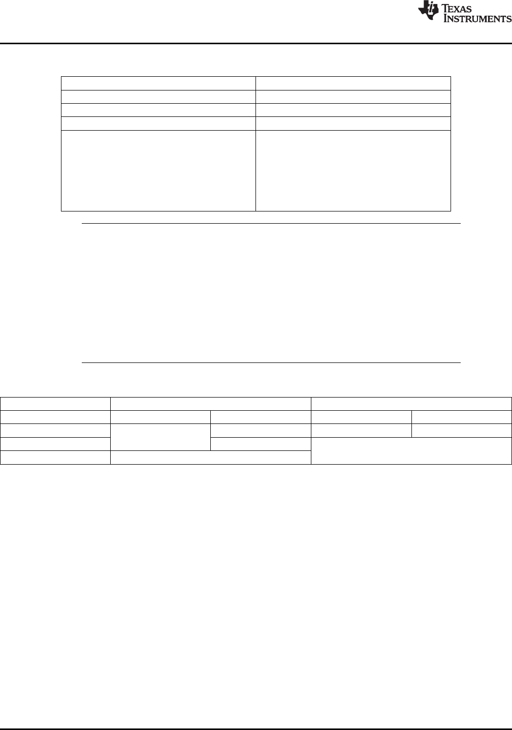
Table 3-4. Addresses of Flash Sectors in F2801, F28015, F28016
ADDRESS RANGE PROGRAM AND DATA SPACE
0x3F 4000 – 0x3F 4FFF Sector D (4K x 16)
0x3F 5000 – 0x3F 5FFF Sector C (4K x 16)
0x3F 6000 – 0x3F 6FFF Sector B (4K x 16)
0x3F 7000 – 0x3F 7F7F Sector A (4K x 16)
0x3F 7F80 – 0x3F 7FF5 Program to 0x0000 when using the
Code Security Module
0x3F 7FF6 – 0x3F 7FF7 Boot-to-Flash Entry Point
(program branch instruction here)
0x3F 7FF8 – 0x3F 7FFF Security Password (128-Bit)
(Do not program to all zeros)
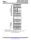
NOTE
• When the code-security passwords are programmed, all addresses between
0x3F7F80 and 0x3F7FF5 cannot be used as program code or data. These locations
must be programmed to 0x0000.
• If the code security feature is not used, addresses 0x3F7F80 through 0x3F7FEF may
be used for code or data. Addresses 0x3F7FF0 – 0x3F7FF5 are reserved for data and
should not contain program code. .
• On ROM devices, addresses 0x3F7FF0 – 0x3F7FF5 and 0x3D7BFC – 0x3D7BFF are
reserved for TI, irrespective of whether code security has been used or not. User
application should not use these locations in any way.
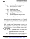
Table 3-5 shows how to handle these memory locations.
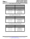
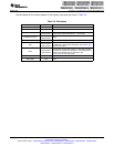
Table 3-5. Impact of Using the Code Security Module
ADDRESS FLASH ROM
Code security enabled Code security disabled Code security enabled Code security disabled
0x3F7F80 – 0x3F7FEF Application code and data Fill with 0x0000 Application code and data
Fill with 0x0000
0x3F7FF0 – 0x3F7FF5 Reserved for data only
Reserved for TI. Do not use.
0x3D7BFC – 0x3D7BFF Application code and data
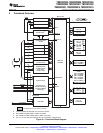
Peripheral Frame 1 and Peripheral Frame 2 are grouped together so as to enable these blocks to be
write/read peripheral block protected. The protected mode ensures that all accesses to these blocks
happen as written. Because of the C28x pipeline, a write immediately followed by a read, to different
memory locations, will appear in reverse order on the memory bus of the CPU. This can cause problems
in certain peripheral applications where the user expected the write to occur first (as written). The C28x
CPU supports a block protection mode where a region of memory can be protected so as to make sure
that operations occur as written (the penalty is extra cycles are added to align the operations). This mode
is programmable and by default, it will protect the selected zones.
32 Functional Overview Copyright © 2003–2009, Texas Instruments Incorporated
Submit Documentation Feedback
Product Folder Link(s): TMS320F2809 TMS320F2808 TMS320F2806 TMS320F2802 TMS320F2801 TMS320C2802
TMS320C2801 TMS320F28016 TMS320F28015