


TMS320F2809, TMS320F2808, TMS320F2806
TMS320F2802, TMS320F2801, TMS320C2802
TMS320C2801, TMS320F28016, TMS320F28015
www.ti.com
SPRS230L–OCTOBER 2003–REVISED DECEMBER 2009
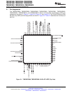
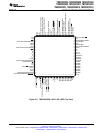
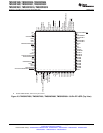
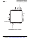
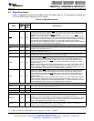
2.2 Signal Descriptions
Table 2-3 describes the signals on the 280x devices. All digital inputs are TTL-compatible. All outputs are
3.3 V with CMOS levels. Inputs are not 5-V tolerant.
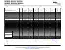
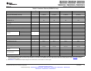
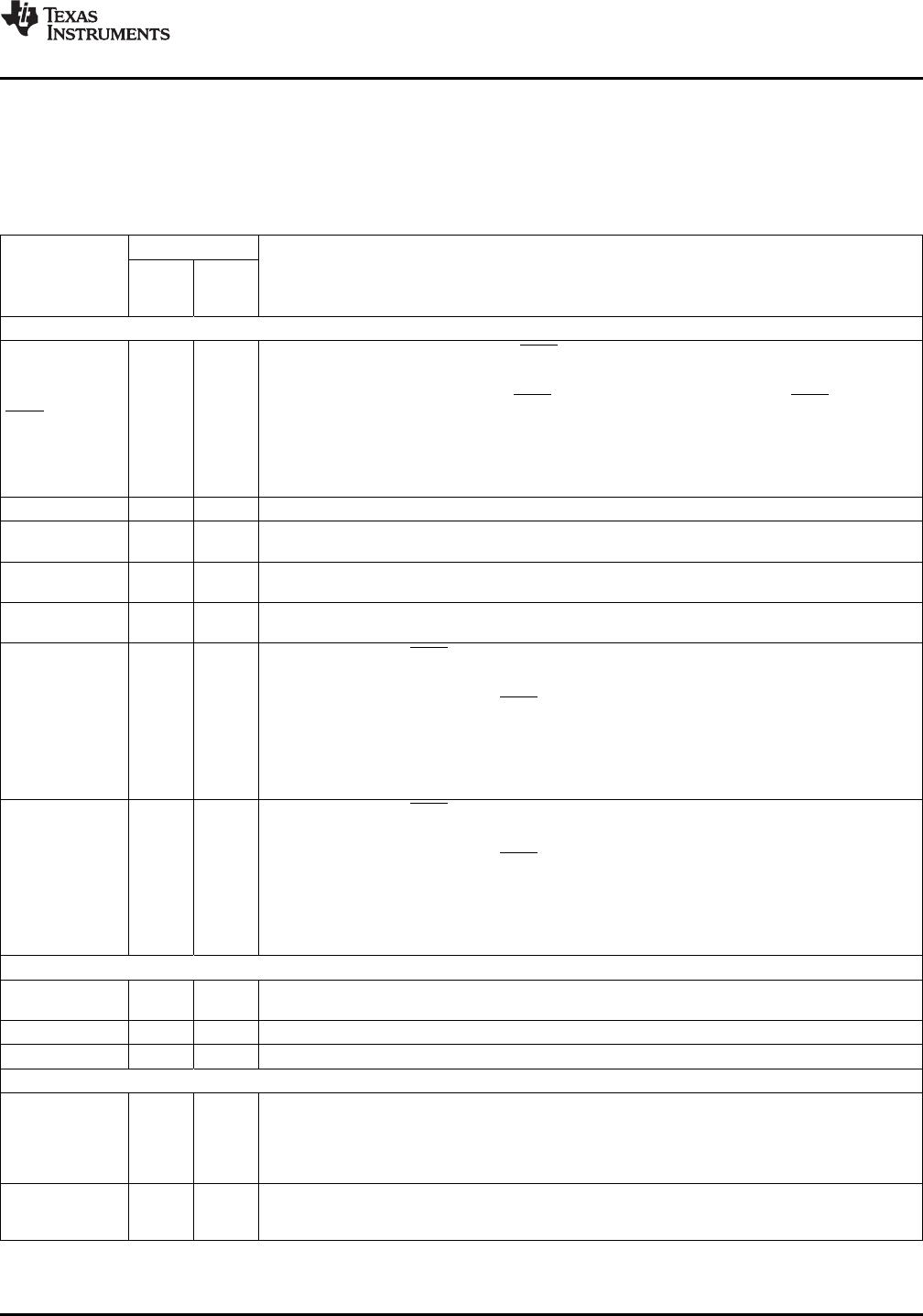
Table 2-3. Signal Descriptions
PIN NO.
GGM/
NAME DESCRIPTION
(1)
PZ
ZGM
PIN #
BALL #
JTAG
JTAG test reset with internal pulldown. TRST, when driven high, gives the scan system control of
the operations of the device. If this signal is not connected or driven low, the device operates in its
functional mode, and the test reset signals are ignored.
NOTE: Do not use pullup resistors on TRST; it has an internal pull-down device. TRST is an active
TRST 84 A6 high test pin and must be maintained low at all times during normal device operation. An external
pulldown resistor is required on this pin. The value of this resistor should be based on drive strength
of the debugger pods applicable to the design. A 2.2-kΩ resistor generally offers adequate
protection. Since this is application-specific, it is recommended that each target board be validated
for proper operation of the debugger and the application. (I, ↓)
TCK 75 A10 JTAG test clock with internal pullup (I, ↑)
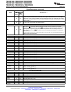
JTAG test-mode select (TMS) with internal pullup. This serial control input is clocked into the TAP
TMS 74 B10
controller on the rising edge of TCK. (I, ↑)
JTAG test data input (TDI) with internal pullup. TDI is clocked into the selected register (instruction
TDI 73 C9
or data) on a rising edge of TCK. (I, ↑)
JTAG scan out, test data output (TDO). The contents of the selected register (instruction or data)
TDO 76 B9
are shifted out of TDO on the falling edge of TCK. (O/Z 8 mA drive)
Emulator pin 0. When TRST is driven high, this pin is used as an interrupt to or from the emulator
system and is defined as input/output through the JTAG scan. This pin is also used to put the
device into boundary-scan mode. With the EMU0 pin at a logic-high state and the EMU1 pin at a
logic-low state, a rising edge on the TRST pin would latch the device into boundary-scan mode.
EMU0 80 A8 (I/O/Z, 8 mA drive ↑)
NOTE: An external pullup resistor is recommended on this pin. The value of this resistor should be
based on the drive strength of the debugger pods applicable to the design. A 2.2-kΩ to 4.7-kΩ
resistor is generally adequate. Since this is application-specific, it is recommended that each target
board be validated for proper operation of the debugger and the application.
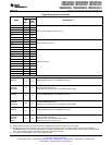
Emulator pin 1. When TRST is driven high, this pin is used as an interrupt to or from the emulator
system and is defined as input/output through the JTAG scan. This pin is also used to put the
device into boundary-scan mode. With the EMU0 pin at a logic-high state and the EMU1 pin at a
logic-low state, a rising edge on the TRST pin would latch the device into boundary-scan mode.
EMU1 81 B7 (I/O/Z, 8 mA drive ↑)
NOTE: An external pullup resistor is recommended on this pin. The value of this resistor should be
based on the drive strength of the debugger pods applicable to the design. A 2.2-kΩ to 4.7-kΩ
resistor is generally adequate. Since this is application-specific, it is recommended that each target
board be validated for proper operation of the debugger and the application.
FLASH
3.3-V Flash Core Power Pin. This pin should be connected to 3.3 V at all times. On the ROM
V
DD3VFL
96 C4
parts (C280x), this pin should be connected to V
DDIO
.
TEST1 97 A3 Test Pin. Reserved for TI. Must be left unconnected. (I/O)
TEST2 98 B3 Test Pin. Reserved for TI. Must be left unconnected. (I/O)
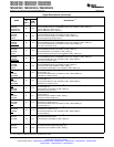
CLOCK
Output clock derived from SYSCLKOUT. XCLKOUT is either the same frequency, one-half the
frequency, or one-fourth the frequency of SYSCLKOUT. This is controlled by the bits 1, 0
XCLKOUT 66 E8 (XCLKOUTDIV) in the XCLK register. At reset, XCLKOUT = SYSCLKOUT/4. The XCLKOUT signal
can be turned off by setting XCLKOUTDIV to 3. Unlike other GPIO pins, the XCLKOUT pin is not
placed in high-impedance state during a reset. (O/Z, 8 mA drive).
External Oscillator Input. This pin is used to feed a clock from an external 3.3-V oscillator. In this
XCLKIN 90 B5 case, tie the X1 pin to GND. Alternately, when a crystal/resonator is used (or if an external 1.8-V
oscillator is fed into the X1 pin), tie the XCLKIN pin to GND. (I)
(1) I = Input, O = Output, Z = High impedance, OD = Open drain, ↑ = Pullup, ↓ = Pulldown
Copyright © 2003–2009, Texas Instruments Incorporated Introduction 19
Submit Documentation Feedback
Product Folder Link(s): TMS320F2809 TMS320F2808 TMS320F2806 TMS320F2802 TMS320F2801 TMS320C2802
TMS320C2801 TMS320F28016 TMS320F28015