


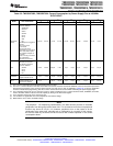
Transmission Line
4.0 pF 1.85 pF
Z0 = 50 Ω
(Α)
Tester Pin Electronics
Data Sheet Timing Reference Point
Output
Under
Test
42 Ω 3.5 nH
Device Pin
(B)
TMS320F2809, TMS320F2808, TMS320F2806
TMS320F2802, TMS320F2801, TMS320C2802
TMS320C2801, TMS320F28016, TMS320F28015
www.ti.com
SPRS230L–OCTOBER 2003–REVISED DECEMBER 2009
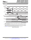
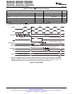
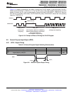
6.6 Timing Parameter Symbology
Timing parameter symbols used are created in accordance with JEDEC Standard 100. To shorten the
symbols, some of the pin names and other related terminology have been abbreviated as follows:
Lowercase subscripts and their Letters and symbols and their
meanings: meanings:
a access time H High
c cycle time (period) L Low
d delay time V Valid
Unknown, changing, or don't care
f fall time X
level
h hold time Z High impedance
r rise time
su setup time
t transition time
v valid time
w pulse duration (width)
6.6.1 General Notes on Timing Parameters
All output signals from the 28x devices (including XCLKOUT) are derived from an internal clock such that
all output transitions for a given half-cycle occur with a minimum of skewing relative to each other.
The signal combinations shown in the following timing diagrams may not necessarily represent actual
cycles. For actual cycle examples, see the appropriate cycle description section of this document.
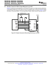
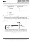
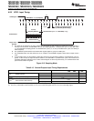
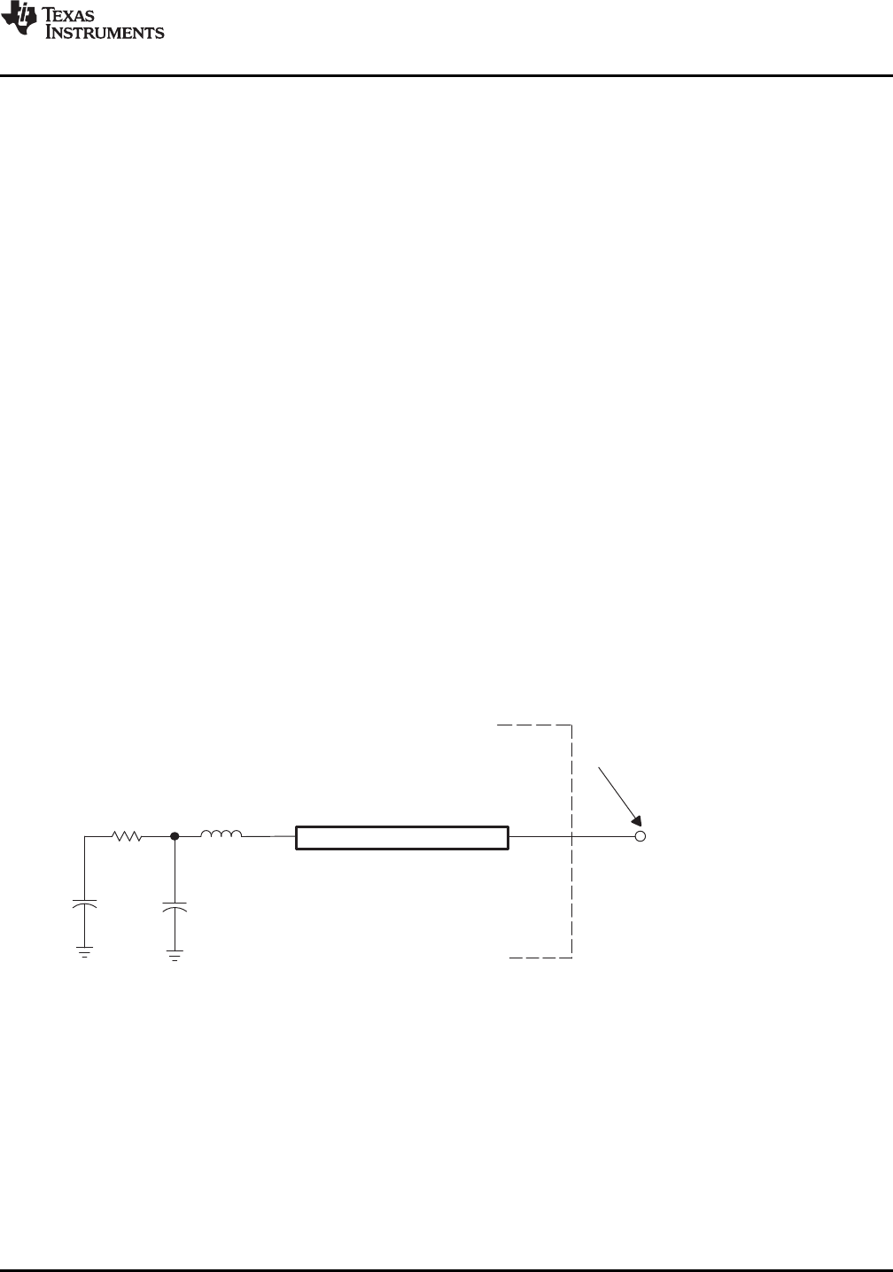
6.6.2 Test Load Circuit
This test load circuit is used to measure all switching characteristics provided in this document.
A. Input requirements in this data sheet are tested with an input slew rate of < 4 Volts per nanosecond (4 V/ns) at the
device pin.
B. The data sheet provides timing at the device pin. For output timing analysis, the tester pin electronics and its
transmission line effects must be taken into account. A transmission line with a delay of 2 ns or longer can be used to
produce the desired transmission line effect. The transmission line is intended as a load only. It is not necessary to
add or subtract the transmission line delay (2 ns or longer) from the data sheet timing.
Figure 6-6. 3.3-V Test Load Circuit
Copyright © 2003–2009, Texas Instruments Incorporated Electrical Specifications 103
Submit Documentation Feedback
Product Folder Link(s): TMS320F2809 TMS320F2808 TMS320F2806 TMS320F2802 TMS320F2801 TMS320C2802
TMS320C2801 TMS320F28016 TMS320F28015